KIT35XS3400EVBE Freescale Semiconductor, KIT35XS3400EVBE Datasheet - Page 14
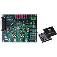
KIT35XS3400EVBE
Manufacturer Part Number
KIT35XS3400EVBE
Description
KIT EVALUATION FOR MC35XS3400
Manufacturer
Freescale Semiconductor
Specifications of KIT35XS3400EVBE
Main Purpose
Automotive Lighting
Utilized Ic / Part
*
Primary Attributes
4 protected high-side switches
Secondary Attributes
SPI Interface
Silicon Manufacturer
Freescale
Silicon Core Number
MC35XS3400
Kit Application Type
Power Management
Application Sub Type
EXtreme Switch
Kit Contents
Evaluation Board, CD
Rohs Compliant
Yes
Lead Free Status / RoHS Status
Lead free / RoHS Compliant
Embedded
-
Lead Free Status / Rohs Status
Lead free / RoHS Compliant


Table 5. Dynamic Electrical Characteristics (continued)
otherwise noted. Typical values noted reflect the approximate parameter means at T
otherwise noted.
14
PWM MODULE TIMING
Notes
35XS3400
ELECTRICAL CHARACTERISTICS
DYNAMIC ELECTRICAL CHARACTERISTICS
Bulb Cooling Time Step
Input PWM Clock Range on IN0
Input PWM Clock Low Frequency Detection Range on IN0
Input PWM Clock High Frequency Detection Range on IN0
Output PWM Frequency Range
Output PWM Frequency Accuracy using Calibrated Oscillator
Default Output PWM Frequency using Internal Oscillator
CS
CS
Output PWM Duty-cycle Range for f
Output PWM Duty-cycle Range for f
Output PWM Duty-cycle Range for f
INPUT TIMING
Direct Input Toggle Timeout
AUTORETRY TIMING
Autoretry Period
33.
34.
Characteristics noted under conditions 6.0 V ≤ V
Calibration Low Minimum Time Detection Range
Calibration Low Maximum Tine Detection Range
Clock Fail detector available for PWM_en bit is set to logic [1] and CLOCK_sel is set to logic [0].
The PWM ratio is measured at V
100%) and fully-off (duty-cycle 0%). For values outside this range, a calibration is needed between the PWM duty-cycle programming
and the PWM on the output with R
CB[1:0]=00 or 11 (medium)
CB[1:0]=01 (fast)
CB[1:0]=10 (slow)
Characteristic
PWM
PWM
PWM
HS
= 1.0 kHz for high speed slew rate
L
= 400 Hz
= 200 Hz
= 50% of V
= 5.0 Ω resistive load.
(34)
(34)
PWR
PWR
and for the default SR value. It is possible to put the device fully-on (PWM duty-cycle
(33)
(33)
≤ 20 V, 3.0 V ≤ V
(34)
A
R
R
t
f
t
R
DD
f
FPWM(CAL)
CSB(MAX)
Symbol
IN0(HIGH)
IN0(LOW)
CSB(MIN)
PWM
PWM
f
t
t
t
t
t
t
t
t
t
t
t
t
t
t
t
t
t
t
PWM
PWM(0)
t
BC1_00
B
B
B
B
B
B
B
B
B
B
BC6_01
B
B
B
B
B
B
f
AUTO
PWM
f
C2_00
C3_00
C4_00
C5_00
C6_00
C1_01
C2_01
C3_01
C4_01
C5_01
C1_10
C2_10
C3_10
C4_10
C5_10
C6_10
t
≤ 5.5 V, - 40°C ≤ T
IN0
IN
_400
_200
_1k
A
= 25°C under nominal conditions, unless
1166
1002
1256
7.68
Min
582
312
356
416
502
628
296
156
176
202
256
452
624
714
834
100
140
175
105
-10
1.0
5.0
6.0
84
14
10
–
Analog Integrated Circuit Device Data
A
≤ 125°C, GND = 0 V, unless
1668
1022
1192
1434
1796
Typ
834
448
510
596
718
898
418
224
254
290
360
648
894
200
120
200
250
150
2.0
20
–
–
–
–
–
–
Freescale Semiconductor
30.72
1084
1168
2170
1164
1310
1552
1866
2340
Max
584
664
776
934
544
292
332
378
468
884
400
+10
156
260
325
195
4.0
1.0
26
98
98
94
Unit
kHz
kHz
kHz
kHz
ms
ms
ms
Hz
μs
μs
%
%
%
%
Related parts for KIT35XS3400EVBE
Image
Part Number
Description
Manufacturer
Datasheet
Request
R

Part Number:
Description:
Manufacturer:
Freescale Semiconductor, Inc
Datasheet:
Part Number:
Description:
Manufacturer:
Freescale Semiconductor, Inc
Datasheet:
Part Number:
Description:
Manufacturer:
Freescale Semiconductor, Inc
Datasheet:
Part Number:
Description:
Manufacturer:
Freescale Semiconductor, Inc
Datasheet:
Part Number:
Description:
Manufacturer:
Freescale Semiconductor, Inc
Datasheet:
Part Number:
Description:
Manufacturer:
Freescale Semiconductor, Inc
Datasheet:
Part Number:
Description:
Manufacturer:
Freescale Semiconductor, Inc
Datasheet:
Part Number:
Description:
Manufacturer:
Freescale Semiconductor, Inc
Datasheet:
Part Number:
Description:
Manufacturer:
Freescale Semiconductor, Inc
Datasheet:
Part Number:
Description:
Manufacturer:
Freescale Semiconductor, Inc
Datasheet:
Part Number:
Description:
Manufacturer:
Freescale Semiconductor, Inc
Datasheet:
Part Number:
Description:
Manufacturer:
Freescale Semiconductor, Inc
Datasheet:
Part Number:
Description:
Manufacturer:
Freescale Semiconductor, Inc
Datasheet:
Part Number:
Description:
Manufacturer:
Freescale Semiconductor, Inc
Datasheet:
Part Number:
Description:
Manufacturer:
Freescale Semiconductor, Inc
Datasheet: