KIT35XS3400EVBE Freescale Semiconductor, KIT35XS3400EVBE Datasheet - Page 36
KIT35XS3400EVBE
Manufacturer Part Number
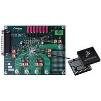
KIT35XS3400EVBE
Description
KIT EVALUATION FOR MC35XS3400
Manufacturer
Freescale Semiconductor
Specifications of KIT35XS3400EVBE
Main Purpose
Automotive Lighting
Utilized Ic / Part
*
Primary Attributes
4 protected high-side switches
Secondary Attributes
SPI Interface
Silicon Manufacturer
Freescale
Silicon Core Number
MC35XS3400
Kit Application Type
Power Management
Application Sub Type
EXtreme Switch
Kit Contents
Evaluation Board, CD
Rohs Compliant
Yes
Lead Free Status / RoHS Status
Lead free / RoHS Compliant
Embedded
-
Lead Free Status / Rohs Status
Lead free / RoHS Compliant


PREVIOUS ADDRESS SOA4 : SOA0 = A
(PWMR_S)
PWMR register for the output selected with A
PREVIOUS ADDRESS SOA4 : SOA0 = A
(CONFR0_S)
CONFR0 register for the output selected with A
PREVIOUS ADDRESS SOA4 : SOA0 = A
(CONFR1_S)
CONFR1 register for the output selected with A
PREVIOUS ADDRESS SOA4 : SOA0 = A
(OCR_S)
OCR register for the output selected with A
PREVIOUS ADDRESS SOA4 : SOA0 = 00101 (GCR)
GCR register.
PREVIOUS ADDRESS SOA4 : SOA0 = 00111
(DIAGR0)
clock on IN0 pin is out of specified frequency range.
calibration failure.
temperature prewarning (temperature of GND flag is above
T
36
35XS3400
FUNCTIONAL DEVICE OPERATION
LOGIC COMMANDS AND REGISTERS
OTWAR
The returned data contains the programmed values in the
The returned data contains the programmed values in the
The returned data contains the programmed values in the
The returned data contains the programmed values in the
The returned data contains the programmed values in the
The returned data OD2 reports logic [1] in case of PWM
The returned data OD1 reports logic [1] in case of
The returned data OD0 reports logic [1] in case of over-
).
1
A
1
1
1
1
1
0
A
A
A
A
A
.
1
1
0
0
0
A
0
A
0
.
001
010
011
100
0
0
.
.
PREVIOUS ADDRESS SOA4 : SOA0 = 01111
(DIAGR1)
of the direct input IN[3:0].
[1]) or not (set to logic [0]). OD4:OD1 report the output state
in case of Fail-safe state due to watchdog time-out as
explained in the following
PREVIOUS ADDRESS SOA4 : SOA0 = 10111
(DIAGR2)
to 1XX for Protected Quad 35 mΩ High Side Switches.
DEFAULT DEVICE CONFIGURATION
• HS output is commanded by corresponding IN input or On
• HS output is fully protected by the severe short-circuit
• Open-load in ON and OFF state and HS shorted to VPWR
• No current recopy and no analog temperature feedback
• Over-voltage protection is enabled,
• SO reporting fault status from HS0,
• VDD failure detection is disabled.
Table 24. Watchdog activation report
The returned data OD4: OD1 report in real time the state
The OD0 indicates if the watchdog is enabled (set to logic
The returned data is the product ID. Bits OD2:OD0 are set
bit through SPI. The medium slew-rate is used,
protection, the under-voltage, and the over-temperature
protection. The auto-retry feature is enabled,
detections are available,
active,
WD_en (OD0)
The default device configuration is explained below:
0
1
Analog Integrated Circuit Device Data
Table
24.
Freescale Semiconductor
disabled
enabled
Related parts for KIT35XS3400EVBE
Image
Part Number
Description
Manufacturer
Datasheet
Request
R

Part Number:
Description:
Manufacturer:
Freescale Semiconductor, Inc
Datasheet:
Part Number:
Description:
Manufacturer:
Freescale Semiconductor, Inc
Datasheet:
Part Number:
Description:
Manufacturer:
Freescale Semiconductor, Inc
Datasheet:
Part Number:
Description:
Manufacturer:
Freescale Semiconductor, Inc
Datasheet:
Part Number:
Description:
Manufacturer:
Freescale Semiconductor, Inc
Datasheet:
Part Number:
Description:
Manufacturer:
Freescale Semiconductor, Inc
Datasheet:
Part Number:
Description:
Manufacturer:
Freescale Semiconductor, Inc
Datasheet:
Part Number:
Description:
Manufacturer:
Freescale Semiconductor, Inc
Datasheet:
Part Number:
Description:
Manufacturer:
Freescale Semiconductor, Inc
Datasheet:
Part Number:
Description:
Manufacturer:
Freescale Semiconductor, Inc
Datasheet:
Part Number:
Description:
Manufacturer:
Freescale Semiconductor, Inc
Datasheet:
Part Number:
Description:
Manufacturer:
Freescale Semiconductor, Inc
Datasheet:
Part Number:
Description:
Manufacturer:
Freescale Semiconductor, Inc
Datasheet:
Part Number:
Description:
Manufacturer:
Freescale Semiconductor, Inc
Datasheet:
Part Number:
Description:
Manufacturer:
Freescale Semiconductor, Inc
Datasheet: