KIT35XS3400EVBE Freescale Semiconductor, KIT35XS3400EVBE Datasheet - Page 24
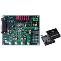
KIT35XS3400EVBE
Manufacturer Part Number
KIT35XS3400EVBE
Description
KIT EVALUATION FOR MC35XS3400
Manufacturer
Freescale Semiconductor
Specifications of KIT35XS3400EVBE
Main Purpose
Automotive Lighting
Utilized Ic / Part
*
Primary Attributes
4 protected high-side switches
Secondary Attributes
SPI Interface
Silicon Manufacturer
Freescale
Silicon Core Number
MC35XS3400
Kit Application Type
Power Management
Application Sub Type
EXtreme Switch
Kit Contents
Evaluation Board, CD
Rohs Compliant
Yes
Lead Free Status / RoHS Status
Lead free / RoHS Compliant
Embedded
-
Lead Free Status / Rohs Status
Lead free / RoHS Compliant


NORMAL MODE
the outputs HS[0:3] are under control, as defined by hson
signal:
hson[x] = ( ( (IN[x] and DIR_dis[x]) or On bit[x] ) and PWM_en
) or (On bit [x] and Duty_cycle[x] and PWM_en).
depends on fault_control signal, as defined below:
fault_control[x] = ( (IN_ON[x] and DIR_dis[x]) and PWM_en )
or (On bit [x]).
Programmable PWM module
PWM module if PWM_en and On bits are set to logic [1].
clock is the factor 2
(CLOCK_sel bit). The outputs HS[0:3] can be controlled in
the range of 5% to 98% with a resolution of 7 bits of duty cycle
(Table
delay (number of PWM clock rising edges) to improve overall
EMC behavior of the light module
24
35XS3400
FUNCTIONAL DEVICE OPERATION
OPERATIONAL MODES
The 35XS3400 is in Normal mode when:
• V
• wake-up = 1,
• fail = 0,
• fault = 0.
In this mode, the NM bit is set to lfault_contrologic [1] and
In this mode and also in Fail-safe, the fault condition reset
The outputs HS[0:3] are controlled by the programmable
The clock frequency from IN0 input pin or from internal
The timing includes seven programmable PWM switching
Table 7. Output PWM Resolution
PWR
7). The state of other IN pin is ignored.
On bit
0
1
1
1
1
1
and V
Duty cycle
DD
0000000
0000001
0000010
1111111
7
are within the normal voltage range,
(128) of the output PWM frequency
X
n
PWM ((n+1)/128 duty cycle)
PWM (1/128 duty cycle)
PWM (2/128 duty cycle)
PWM (3/128 duty cycle)
(Table
Output state
fully ON
OFF
8).
order to report a clock failure in case of the frequency is out
a specified frequency range (from f
case of clock failure, no PWM feature is provided, the On bit
defines the outputs state and the CLOCK_fail bit reports [1].
Calibratable internal clock
corresponding to typical f
reference already available to the MCU, the 35XS3400
allows clock period setting within ±10 percent of accuracy.
Calibrating the internal clock is initiated by defined word to
CALR register. The calibration pulse is provided by the MCU.
The pulse is sent on the
launched. At the moment, the
to [0] until from logic [0] to [1] determine the period of internal
clock with a multiplicative factor of 128.
range (from t
be ignored and the internal clock will be unaltered or reset to
default value (f
IN0 input, when CLOCK_sel is set to [1].
The clock frequency from IN0 is permanently monitored in
The internal clock can vary as much as +/-30 percent
Using the existing SPI inputs and the precision timing
In case of negative
The calibratable clock is used, instead of the clock from
Table 8. Output PWM Switching Delay
CS
SI
Delay bits
000
001
010
011
100
101
110
111
CSB(MIN)
CALR
PWM(0)
) if this was not calibrated before.
to t
CS
Analog Integrated Circuit Device Data
CS
CSB(MAX)
PWM(0)
pulse is outside a predefined time
pin after the SPI word is
clock duration
112 PWM clock periods
CS
16 PWM clock periods
32 PWM clock periods
48 PWM clock periods
64 PWM clock periods
80 PWM clock periods
96 PWM clock periods
SI command
Internal
output switching period.
ignored
pin transitions from logic [1]
), the calibration event will
Output delay
Freescale Semiconductor
IN0(LOW)
no delay
to f
IN0(HIGH)
). In
Related parts for KIT35XS3400EVBE
Image
Part Number
Description
Manufacturer
Datasheet
Request
R

Part Number:
Description:
Manufacturer:
Freescale Semiconductor, Inc
Datasheet:
Part Number:
Description:
Manufacturer:
Freescale Semiconductor, Inc
Datasheet:
Part Number:
Description:
Manufacturer:
Freescale Semiconductor, Inc
Datasheet:
Part Number:
Description:
Manufacturer:
Freescale Semiconductor, Inc
Datasheet:
Part Number:
Description:
Manufacturer:
Freescale Semiconductor, Inc
Datasheet:
Part Number:
Description:
Manufacturer:
Freescale Semiconductor, Inc
Datasheet:
Part Number:
Description:
Manufacturer:
Freescale Semiconductor, Inc
Datasheet:
Part Number:
Description:
Manufacturer:
Freescale Semiconductor, Inc
Datasheet:
Part Number:
Description:
Manufacturer:
Freescale Semiconductor, Inc
Datasheet:
Part Number:
Description:
Manufacturer:
Freescale Semiconductor, Inc
Datasheet:
Part Number:
Description:
Manufacturer:
Freescale Semiconductor, Inc
Datasheet:
Part Number:
Description:
Manufacturer:
Freescale Semiconductor, Inc
Datasheet:
Part Number:
Description:
Manufacturer:
Freescale Semiconductor, Inc
Datasheet:
Part Number:
Description:
Manufacturer:
Freescale Semiconductor, Inc
Datasheet:
Part Number:
Description:
Manufacturer:
Freescale Semiconductor, Inc
Datasheet: