KIT35XS3400EVBE Freescale Semiconductor, KIT35XS3400EVBE Datasheet - Page 7
KIT35XS3400EVBE
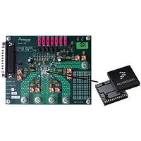
Manufacturer Part Number
KIT35XS3400EVBE
Description
KIT EVALUATION FOR MC35XS3400
Manufacturer
Freescale Semiconductor
Specifications of KIT35XS3400EVBE
Main Purpose
Automotive Lighting
Utilized Ic / Part
*
Primary Attributes
4 protected high-side switches
Secondary Attributes
SPI Interface
Silicon Manufacturer
Freescale
Silicon Core Number
MC35XS3400
Kit Application Type
Power Management
Application Sub Type
EXtreme Switch
Kit Contents
Evaluation Board, CD
Rohs Compliant
Yes
Lead Free Status / RoHS Status
Lead free / RoHS Compliant
Embedded
-
Lead Free Status / Rohs Status
Lead free / RoHS Compliant


Table 4. Static Electrical Characteristics
otherwise noted. Typical values noted reflect the approximate parameter means at T
otherwise noted.
Analog Integrated Circuit Device Data
Freescale Semiconductor
POWER INPUTS
OUTPUTS HS0 TO HS3
Notes
Battery Supply Voltage Range
Battery Clamp Voltage
V
Sleep State Supply Current
V
V
V
Over-voltage Shutdown Threshold
Over-voltage Shutdown Hysteresis
Under-voltage Shutdown Threshold
V
V
Recovery Under-voltage Threshold
Output Drain-to-Source ON Resistance
V
10.
11.
12.
13.
Characteristics noted under conditions 6.0 V ≤ V
PWR
DD
DD
DD
PWR
DD
PWR
Fully Operational
Extended mode
Outputs commanded ON,
Outputs commanded OFF, OFF Open-load Detection Disabled,
HS[0 : 3] shorted to the ground with V
WAKE > V
T
T
No SPI Communication
8.0 MHz SPI Communication
V
V
V
V
V
ground
A
A
PWR
PWR
PWR
PWR
PWR
Supply Voltage
Supply Current at V
Sleep State Current at V
Supply Failure Threshold ( for
= 25°C
= 85°C
In extended mode, the functionality is guaranteed but not the electrical parameters. From 4.0 V to 6.0 V voltage range, the device is only
protected with the thermal shutdown detection.
Measured with the outputs open.
Typical value guaranteed per design.
Output will automatically recover with time limited autoretry to instructed state when V
V
supplied by V
Operating Supply Current
and V
Supply Current
PWR
= 4.0 V
= 6.0 V
= 10 V
= 13 V
= 12 V,
DD
degradation level did not go below the under-voltage power-ON reset threshold. This applies to all internal device logic that is
IH
Power on Reset Threshold
or
RST
(10)
RST
PWR
(11)
= WAKE = IN[0:3] < V
> V
DD
and assumes that the external V
Characteristic
IH
= 5.5 V
HS[0 : 3] open,
DD
and IN[0:3] < V
(12)
= 5.5 V
V
(13)
PWR
(
I
STATIC ELECTRICAL CHARACTERISTICS
HS
DD
> V
IL
= 2.0 A, T
IL
IN[0:3] > V
= 5.5 V
,
PWR(UV)
HS[0 : 3] shorted to the
A
)
PWR
IH
= 25
DD
supply is within specification.
°
≤ 20 V, 3.0 V ≤ V
C)
V
V
V
V
I
SUPPLY(POR)
R
PWR(SLEEP)
PWR(CLAMP)
I
PWR(OVHYS)
PWR(UV)_UP
I
V
V
I
DD(SLEEP)
V
PWR(SBY)
V
DS(ON)_25
Symbol
PWR(ON)
I
PWR(OV)
PWR(UV)
DD(FAIL)
DD(ON)
V
DD(ON)
PWR
DD
≤ 5.5 V, - 40°C ≤ T
PWR
A
Min
= 25°C under nominal conditions, unless
6.0
4.0
3.0
0.2
3.3
0.5
2.2
3.4
41
28
STATIC ELECTRICAL CHARACTERISTICS
–
–
–
–
–
–
–
–
–
–
–
voltage is restored to normal as long as the
A
ELECTRICAL CHARACTERISTICS
≤ 125°C, GND = 0 V, unless
Typ
6.5
6.0
1.0
1.6
5.0
0.8
3.9
2.5
4.1
47
32
–
–
–
–
–
–
–
–
–
–
Max
100
8.0
5.0
5.5
2.2
5.0
1.5
4.3
0.9
2.8
4.5
20
28
53
20
30
36
55
35
35
–
V
35XS3400
PWR(UV)
Unit
mA
mA
mA
mΩ
μA
μA
V
V
V
V
V
V
V
V
7
Related parts for KIT35XS3400EVBE
Image
Part Number
Description
Manufacturer
Datasheet
Request
R

Part Number:
Description:
Manufacturer:
Freescale Semiconductor, Inc
Datasheet:
Part Number:
Description:
Manufacturer:
Freescale Semiconductor, Inc
Datasheet:
Part Number:
Description:
Manufacturer:
Freescale Semiconductor, Inc
Datasheet:
Part Number:
Description:
Manufacturer:
Freescale Semiconductor, Inc
Datasheet:
Part Number:
Description:
Manufacturer:
Freescale Semiconductor, Inc
Datasheet:
Part Number:
Description:
Manufacturer:
Freescale Semiconductor, Inc
Datasheet:
Part Number:
Description:
Manufacturer:
Freescale Semiconductor, Inc
Datasheet:
Part Number:
Description:
Manufacturer:
Freescale Semiconductor, Inc
Datasheet:
Part Number:
Description:
Manufacturer:
Freescale Semiconductor, Inc
Datasheet:
Part Number:
Description:
Manufacturer:
Freescale Semiconductor, Inc
Datasheet:
Part Number:
Description:
Manufacturer:
Freescale Semiconductor, Inc
Datasheet:
Part Number:
Description:
Manufacturer:
Freescale Semiconductor, Inc
Datasheet:
Part Number:
Description:
Manufacturer:
Freescale Semiconductor, Inc
Datasheet:
Part Number:
Description:
Manufacturer:
Freescale Semiconductor, Inc
Datasheet:
Part Number:
Description:
Manufacturer:
Freescale Semiconductor, Inc
Datasheet: