EVAL-AD7674CBZ Analog Devices Inc, EVAL-AD7674CBZ Datasheet - Page 23
EVAL-AD7674CBZ
Manufacturer Part Number
EVAL-AD7674CBZ
Description
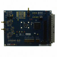
BOARD EVALUATION FOR AD7674
Manufacturer
Analog Devices Inc
Series
PulSAR®r
Specifications of EVAL-AD7674CBZ
Number Of Adc's
1
Number Of Bits
18
Sampling Rate (per Second)
800k
Data Interface
Serial, Parallel
Inputs Per Adc
1 Differential
Input Range
0 ~ 5 V
Power (typ) @ Conditions
126mW @ 800kSPS
Voltage Supply Source
Analog and Digital
Operating Temperature
-40°C ~ 85°C
Utilized Ic / Part
AD7674
Lead Free Status / RoHS Status
Lead free / RoHS Compliant


degradation of the conversion result could occur. This is
particularly important during the second half of the conversion
phase because the AD7674 provides error correction circuitry
that can correct for an improper bit decision made during the
first half of the conversion phase. For this reason, it is
recommended that when an external clock is being provided, it
is a discontinuous clock that only toggles when BUSY is low or,
more importantly, that it does not transition during the latter
half of BUSY high.
External Discontinuous Clock Data Read after
Conversion
Though maximum throughput cannot be achieved using this
mode, it is the most recommended of the serial slave modes.
Figure 42 shows the detailed timing diagrams of this method.
After a conversion is complete, indicated by BUSY returning
low, the result of this conversion can be read while both CS and
RD are low. Data is shifted out MSB first with 18 clock pulses,
and is valid on the rising and falling edge of the clock.
SDOUT
BUSY
SCLK
SDIN
CS
t
t
31
16
t
33
Figure 42. Slave Serial Data Timing for Reading (Read after Convert)
X
t
36
1
t
35
D17
X17
t
37
t
34
2
EXT/INT = 1
X16
D16
t
32
Rev. A | Page 23 of 28
3
X15
D15
INVSCLK = 0
Among the advantages of this method, the conversion
performance is not degraded because there are no voltage
transients on the digital interface during the conversion process.
Also, data can be read at speeds up to 40 MHz, accommodating
both slow digital host interface and the fastest serial reading.
Finally, in this mode only, the AD7674 provides a daisy-chain
feature using the RDC/SDIN input pin to cascade multiple
converters together. This feature is useful for reducing
component count and wiring connections when desired (for
instance, in isolated multiconverter applications).
An example of the concatenation of two devices is shown in
Figure 44. Simultaneous sampling is possible by using a
common CNVST signal. It should be noted that the RDC/SDIN
input is latched on the edge of SCLK opposite the one used to
shift out data on SDOUT. Thus, the MSB of the upstream
converter follows the LSB of the downstream converter on the
next SCLK cycle.
16
17
D1
X1
RD = 0
18
D0
X0
19
X17
Y17
20
03083-0-042
X16
Y16
AD7674
Related parts for EVAL-AD7674CBZ
Image
Part Number
Description
Manufacturer
Datasheet
Request
R


Part Number:
Description:
BOARD EVAL FOR SI270X-A
Manufacturer:
Silicon Laboratories Inc
Datasheet:

Part Number:
Description:
BUCK CONV REF DESIGN KIT IP1201
Manufacturer:
International Rectifier
Datasheet:
Part Number:
Description:
BOARD DEMO SYNC DUAL BUCK CNVTER
Manufacturer:
International Rectifier
Datasheet:
Part Number:
Description:
BOARD DEMO SYNC BUCK CONVETER
Manufacturer:
International Rectifier
Datasheet:

Part Number:
Description:
EVALBOARD/EB Omnidirectional microphone - Analog
Manufacturer:
Analog Devices
Datasheet:
Part Number:
Description:
EVALBOARD/EB Omnidirectional microphone - Analog
Manufacturer:
Analog Devices
Datasheet:


Part Number:
Description:
BOARD EVAL LED DRIVER LT3756
Manufacturer:
Linear Technology
Datasheet:

Part Number:
Description:
BOARD EVAL FOR AD7741/7742
Manufacturer:
Analog Devices Inc
Datasheet:

Part Number:
Description:
±1.7g Dual-Axis IMEMS Accelerometer Evaluation Board
Manufacturer:
Analog Devices Inc
Datasheet:

Part Number:
Description:
IC MULTIPLIER ANALOG 8-SOIC T/R
Manufacturer:
Analog Devices Inc
Datasheet:

Part Number:
Description:
IC ANALOG MULTIPLIER 8-DIP
Manufacturer:
Analog Devices Inc
Datasheet:
Part Number:
Description:
IC ANALOG MULTIPLIER 8-SOIC
Manufacturer:
Analog Devices Inc
Datasheet:
Part Number:
Description:
IC ANALOG MULTIPLIER 8-DIP
Manufacturer:
Analog Devices Inc
Datasheet: