EVAL-AD7674CBZ Analog Devices Inc, EVAL-AD7674CBZ Datasheet - Page 8
EVAL-AD7674CBZ
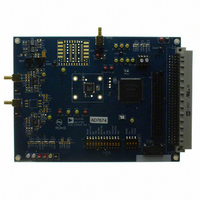
Manufacturer Part Number
EVAL-AD7674CBZ
Description
BOARD EVALUATION FOR AD7674
Manufacturer
Analog Devices Inc
Series
PulSAR®r
Specifications of EVAL-AD7674CBZ
Number Of Adc's
1
Number Of Bits
18
Sampling Rate (per Second)
800k
Data Interface
Serial, Parallel
Inputs Per Adc
1 Differential
Input Range
0 ~ 5 V
Power (typ) @ Conditions
126mW @ 800kSPS
Voltage Supply Source
Analog and Digital
Operating Temperature
-40°C ~ 85°C
Utilized Ic / Part
AD7674
Lead Free Status / RoHS Status
Lead free / RoHS Compliant


AD7674
PIN CONFIGURATION AND FUNCTION DESCRIPTIONS
Table 6. Pin Function Descriptions
Pin No.
1, 44
2, 47
3
4
5
6
7
8
Mnemonic
AGND
AVDD
MODE0
MODE1
D0/OB/2C
WARP
IMPULSE
D1/A0
Type
P
P
DI
DI
DI/O
DI
DI
DI/O
1
Description
Analog Power Ground Pin.
Input Analog Power Pins. Nominally 5 V.
Data Output Interface Mode Selection.
Data Output Interface Mode Selection:
When MODE = 0 (18-bit interface mode), this pin is Bit 0 of the parallel port data output bus and the
data coding is straight binary. In all other modes, this pin allows choice of straight binary/binary twos
complement. When OB/2C is HIGH, the digital output is straight binary; when LOW, the MSB is inverted,
resulting in a twos complement output from its internal shift register.
Conversion Mode Selection. When this input is HIGH and the IMPULSE pin is LOW, WARP selects the
fastest mode, the maximum throughput is achievable, and a minimum conversion rate must be applied
in order to guarantee full specified accuracy. When LOW, full accuracy is maintained independent of the
minimum conversion rate.
Conversion Mode Selection. When this input is HIGH and the WARP pin is LOW, IMPULSE selects a
reduced power mode. In this mode, the power dissipation is approximately proportional to the
sampling rate. When WARP and IMPULSE pins are LOW, the NORMAL mode is selected.
When MODE = 0 (18-bit interface mode), this pin is Bit 1 of the parallel port data output bus. In all other
modes, this input pin controls the form in which data is output, as shown in Table 7.
NOTES
1. NC = NO CONNECT.
2. THE EXPOSED PAD IS INTERNALLY CONNECTED TO AGND. THIS CONNECTION
D4/DIVSCLK[0]
D5/DIVSCLK[1]
Interface MODE
#
0
1
2
3
IS NOT REQUIRED TO MEET THE ELECTRICAL PERFORMANCES HOWEVER, FOR
INCREASED RELIABILITY OF THE SOLDER JOINTS, IT IS RECOMMENDED THAT
THE PAD BE SOLDERED TO THE ANALOG GROUND OF THE SYSTEM.
D0/OB/2C
IMPULSE
MODE0
MODE1
WARP
AGND
AVDD
D1/A0
D2/A1
Figure 4. 48-Lead LQFP and 48-Lead LFCSP (ST-48 and CP-48)
D3
10
11
12
1
2
3
4
5
6
7
8
9
PIN 1
INDICATOR
MODE1
0
0
1
1
Rev. A | Page 8 of 28
(Not to Scale)
AD7674
TOP VIEW
MODE0
0
1
0
1
Description
18-Bit
Interface
16-Bit
Interface
Byte Interface
Serial Interface
36
35
34
33
32
31
30
29
28
27
26
25
AGND
CNVST
PD
RESET
CS
RD
DGND
BUSY
D17
D16
D15
D14
Related parts for EVAL-AD7674CBZ
Image
Part Number
Description
Manufacturer
Datasheet
Request
R


Part Number:
Description:
BOARD EVAL FOR SI270X-A
Manufacturer:
Silicon Laboratories Inc
Datasheet:

Part Number:
Description:
BUCK CONV REF DESIGN KIT IP1201
Manufacturer:
International Rectifier
Datasheet:
Part Number:
Description:
BOARD DEMO SYNC DUAL BUCK CNVTER
Manufacturer:
International Rectifier
Datasheet:
Part Number:
Description:
BOARD DEMO SYNC BUCK CONVETER
Manufacturer:
International Rectifier
Datasheet:

Part Number:
Description:
EVALBOARD/EB Omnidirectional microphone - Analog
Manufacturer:
Analog Devices
Datasheet:
Part Number:
Description:
EVALBOARD/EB Omnidirectional microphone - Analog
Manufacturer:
Analog Devices
Datasheet:


Part Number:
Description:
BOARD EVAL LED DRIVER LT3756
Manufacturer:
Linear Technology
Datasheet:

Part Number:
Description:
BOARD EVAL FOR AD7741/7742
Manufacturer:
Analog Devices Inc
Datasheet:

Part Number:
Description:
±1.7g Dual-Axis IMEMS Accelerometer Evaluation Board
Manufacturer:
Analog Devices Inc
Datasheet:

Part Number:
Description:
IC MULTIPLIER ANALOG 8-SOIC T/R
Manufacturer:
Analog Devices Inc
Datasheet:

Part Number:
Description:
IC ANALOG MULTIPLIER 8-DIP
Manufacturer:
Analog Devices Inc
Datasheet:
Part Number:
Description:
IC ANALOG MULTIPLIER 8-SOIC
Manufacturer:
Analog Devices Inc
Datasheet:
Part Number:
Description:
IC ANALOG MULTIPLIER 8-DIP
Manufacturer:
Analog Devices Inc
Datasheet: