EVAL-AD7674CBZ Analog Devices Inc, EVAL-AD7674CBZ Datasheet - Page 5
EVAL-AD7674CBZ
Manufacturer Part Number
EVAL-AD7674CBZ
Description
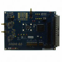
BOARD EVALUATION FOR AD7674
Manufacturer
Analog Devices Inc
Series
PulSAR®r
Specifications of EVAL-AD7674CBZ
Number Of Adc's
1
Number Of Bits
18
Sampling Rate (per Second)
800k
Data Interface
Serial, Parallel
Inputs Per Adc
1 Differential
Input Range
0 ~ 5 V
Power (typ) @ Conditions
126mW @ 800kSPS
Voltage Supply Source
Analog and Digital
Operating Temperature
-40°C ~ 85°C
Utilized Ic / Part
AD7674
Lead Free Status / RoHS Status
Lead free / RoHS Compliant


TIMING SPECIFICATIONS
Table 3. –40°C to +85°C, AVDD = DVDD = 5 V, OVDD = 2.7 V to 5.25 V, unless otherwise noted.
Parameter
Refer to Figure 34 and Figure 35
Refer to Figure 36, Figure 37, and Figure 38 (Parallel Interface Modes)
Refer to Figure 40 and Figure 41 (Master Serial Interface Modes)
Refer to Figure 42 and Figure 43 (Slave Serial Interface Modes)
1
2
3
In Warp mode only, the maximum time between conversions is 1 ms; otherwise, there is no required maximum time.
In serial interface modes, the SYNC, SCLK, and SDOUT timings are defined with a maximum load C
In Serial Master Read during Convert mode. See Table 4 for Serial Master Read after Convert mode.
Convert Pulsewidth
Time between Conversions (Warp Mode/Normal Mode/Impulse Mode)
CNVST LOW to BUSY HIGH Delay
BUSY HIGH All Modes Except Master Serial Read after Convert
Aperture Delay
End of Conversion to BUSY LOW Delay
Conversion Time (Warp Mode/Normal Mode/Impulse Mode)
Acquisition Time
RESET Pulsewidth
CNVST LOW to Data Valid Delay (Warp Mode/Normal Mode/Impulse Mode)
Data Valid to BUSY LOW Delay
Bus Access Request to Data Valid
Bus Relinquish Time
CS LOW to SYNC Valid Delay
CS LOW to Internal SCLK Valid Delay
CS LOW to SDOUT Delay
CNVST LOW to SYNC Delay (Warp Mode/Normal Mode/Impulse Mode)
SYNC Asserted to SCLK First Edge Delay
Internal SCLK Period
Internal SCLK HIGH
Internal SCLK LOW
SDOUT Valid Setup Time
SDOUT Valid Hold Time
SCLK Last Edge to SYNC Delay
CS HIGH to SYNC HI-Z
CS HIGH to Internal SCLK HI-Z
CS HIGH to SDOUT HI-Z
BUSY HIGH in Master Serial Read after Convert
CNVST LOW to SYNC Asserted Delay
SYNC Deasserted to BUSY LOW Delay
External SCLK Setup Time
External SCLK Active Edge to SDOUT Delay
SDIN Setup Time
SDIN Hold Time
External SCLK Period
External SCLK HIGH
External SCLK LOW
(Warp Mode/Normal Mode/Impulse Mode)
(Warp Mode/Normal Mode/Impulse Mode)
3
3
3
3
3
3
3
3
Rev. A | Page 5 of 28
2
1
Symbol
t
t
t
t
t
t
t
t
t
t
t
t
t
t
t
t
t
t
t
t
t
t
t
t
t
t
t
t
t
t
t
t
t
t
t
t
t
1
2
3
4
5
6
7
8
9
10
11
12
13
14
15
16
17
18
19
20
21
22
23
24
25
26
27
28
29
30
31
32
33
34
35
36
37
L
of 10 pF; otherwise, the load is 60 pF maximum.
Min
10
1.25/1.5/1.75
10
250
10
20
5
3
25
12
7
4
2
3
5
3
5
5
25
10
10
Typ
2
25/275/525
Table 4
1/1.25/1.5
25
Max
35
1/1.25/1.5
1/1.25/1.5
1/1.25/1.5
45
15
10
10
10
40
10
10
10
18
AD7674
Unit
ns
μs
ns
μs
ns
ns
μs
ns
ns
μs
ns
ns
ns
ns
ns
ns
ns
ns
ns
ns
ns
ns
ns
ns
ns
ns
μs
ns
ns
ns
ns
ns
ns
ns
ns
Related parts for EVAL-AD7674CBZ
Image
Part Number
Description
Manufacturer
Datasheet
Request
R


Part Number:
Description:
BOARD EVAL FOR SI270X-A
Manufacturer:
Silicon Laboratories Inc
Datasheet:

Part Number:
Description:
BUCK CONV REF DESIGN KIT IP1201
Manufacturer:
International Rectifier
Datasheet:
Part Number:
Description:
BOARD DEMO SYNC DUAL BUCK CNVTER
Manufacturer:
International Rectifier
Datasheet:
Part Number:
Description:
BOARD DEMO SYNC BUCK CONVETER
Manufacturer:
International Rectifier
Datasheet:

Part Number:
Description:
EVALBOARD/EB Omnidirectional microphone - Analog
Manufacturer:
Analog Devices
Datasheet:
Part Number:
Description:
EVALBOARD/EB Omnidirectional microphone - Analog
Manufacturer:
Analog Devices
Datasheet:


Part Number:
Description:
BOARD EVAL LED DRIVER LT3756
Manufacturer:
Linear Technology
Datasheet:

Part Number:
Description:
BOARD EVAL FOR AD7741/7742
Manufacturer:
Analog Devices Inc
Datasheet:

Part Number:
Description:
±1.7g Dual-Axis IMEMS Accelerometer Evaluation Board
Manufacturer:
Analog Devices Inc
Datasheet:

Part Number:
Description:
IC MULTIPLIER ANALOG 8-SOIC T/R
Manufacturer:
Analog Devices Inc
Datasheet:

Part Number:
Description:
IC ANALOG MULTIPLIER 8-DIP
Manufacturer:
Analog Devices Inc
Datasheet:
Part Number:
Description:
IC ANALOG MULTIPLIER 8-SOIC
Manufacturer:
Analog Devices Inc
Datasheet:
Part Number:
Description:
IC ANALOG MULTIPLIER 8-DIP
Manufacturer:
Analog Devices Inc
Datasheet: