EVAL5985 STMicroelectronics, EVAL5985 Datasheet - Page 11
EVAL5985
Manufacturer Part Number
EVAL5985
Description
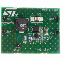
BOARD EVAL FOR L5985
Manufacturer
STMicroelectronics
Type
DC/DC Switching Converters, Regulators & Controllersr
Specifications of EVAL5985
Main Purpose
DC/DC, Step Down
Outputs And Type
1, Non-Isolated
Voltage - Output
3.3V
Current - Output
2A
Voltage - Input
3.3 ~ 18V
Regulator Topology
Buck
Frequency - Switching
500kHz
Board Type
Fully Populated
Utilized Ic / Part
L5985
Input Voltage
2.9 V to 18 V
Output Voltage
0.6 V to 16 V
Product
Power Management Modules
Silicon Manufacturer
ST Micro
Silicon Core Number
L5985
Kit Application Type
Power Management - Voltage Regulator
Application Sub Type
Step Down Switching Regulator
Kit Contents
Board
Lead Free Status / RoHS Status
Lead free / RoHS Compliant
Power - Output
-
Lead Free Status / Rohs Status
Lead free / RoHS Compliant
For Use With/related Products
L5985
Other names
497-6387
EVAL5985
EVAL5985
Available stocks
Company
Part Number
Manufacturer
Quantity
Price


L5985
4.3
Error amplifier and compensation
The error amplifier (E/A) provides the error signal to be compared with the sawtooth to
perform the pulse width modulation. Its non-inverting input is internally connected to a 0.6 V
voltage reference, while its inverting input (FB) and output (COMP) are externally available
for feedback and frequency compensation. In this device the error amplifier is a voltage
mode operational amplifier so with high DC gain and low output impedance.
The uncompensated error amplifier characteristics are the following:
Table 5.
In continuos conduction mode (CCM), the transfer function of the power section has two
poles due to the LC filter and one zero due to the ESR of the output capacitor. Different
kinds of compensation networks can be used depending on the ESR value of the output
capacitor. In case the zero introduced by the output capacitor helps to compensate the
double pole of the LC filter a type II compensation network can be used. Otherwise, a type
III compensation network has to be used (see
compensation network selection).
Anyway the methodology to compensate the loop is to introduce zeros to obtain a safe
phase margin.
Maximum source/sink current
Uncompensated error amplifier characteristics
Output voltage swing
Low frequency gain
Error amplifier
Slew rate
GBWP
Doc ID 13006 Rev 5
Chapter 5.4
for details about the
25 mA/40 mA
0 to 3.3 V
4.5 MHz
100 dB
7 V/μs
Value
Functional description
11/37
Related parts for EVAL5985
Image
Part Number
Description
Manufacturer
Datasheet
Request
R

Part Number:
Description:
STMicroelectronics [RIPPLE-CARRY BINARY COUNTER/DIVIDERS]
Manufacturer:
STMicroelectronics
Datasheet:
Part Number:
Description:
STMicroelectronics [LIQUID-CRYSTAL DISPLAY DRIVERS]
Manufacturer:
STMicroelectronics
Datasheet:

Part Number:
Description:
BOARD EVAL FOR MEMS SENSORS
Manufacturer:
STMicroelectronics
Datasheet:
Part Number:
Description:
NPN TRANSISTOR POWER MODULE
Manufacturer:
STMicroelectronics
Datasheet:
Part Number:
Description:
TURBOSWITCH ULTRA-FAST HIGH VOLTAGE DIODE
Manufacturer:
STMicroelectronics
Datasheet:
Part Number:
Description:
Manufacturer:
STMicroelectronics
Datasheet:
Part Number:
Description:
DIODE / SCR MODULE
Manufacturer:
STMicroelectronics
Datasheet:
Part Number:
Description:
DIODE / SCR MODULE
Manufacturer:
STMicroelectronics
Datasheet:
Part Number:
Description:
Search -----> STE16N100
Manufacturer:
STMicroelectronics
Datasheet:
Part Number:
Description:
Search ---> STE53NA50
Manufacturer:
STMicroelectronics
Datasheet:
Part Number:
Description:
NPN Transistor Power Module
Manufacturer:
STMicroelectronics
Datasheet:
Part Number:
Description:
DIODE / SCR MODULE
Manufacturer:
STMicroelectronics
Datasheet: