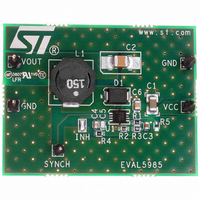
EVAL5985 STMicroelectronics, EVAL5985 Datasheet - Page 26

EVAL5985
Manufacturer Part Number
EVAL5985
Description
BOARD EVAL FOR L5985
Manufacturer
STMicroelectronics
Type
DC/DC Switching Converters, Regulators & Controllersr
Specifications of EVAL5985
Main Purpose
DC/DC, Step Down
Outputs And Type
1, Non-Isolated
Voltage - Output
3.3V
Current - Output
2A
Voltage - Input
3.3 ~ 18V
Regulator Topology
Buck
Frequency - Switching
500kHz
Board Type
Fully Populated
Utilized Ic / Part
L5985
Input Voltage
2.9 V to 18 V
Output Voltage
0.6 V to 16 V
Product
Power Management Modules
Silicon Manufacturer
ST Micro
Silicon Core Number
L5985
Kit Application Type
Power Management - Voltage Regulator
Application Sub Type
Step Down Switching Regulator
Kit Contents
Board
Lead Free Status / RoHS Status
Lead free / RoHS Compliant
Power - Output
-
Lead Free Status / Rohs Status
Lead free / RoHS Compliant
For Use With/related Products
L5985
Other names
497-6387
EVAL5985
EVAL5985
Available stocks
Company
Part Number
Manufacturer
Quantity
Price
Application information
5.5
26/37
Thermal considerations
The thermal design is important to prevent the thermal shutdown of device if junction
temperature goes above 150 °C. The three different sources of losses within the device are:
Equation 27
Where D is the duty cycle of the application and the maximum R
Note that the duty cycle is theoretically given by the ratio between V
it is quite higher to compensate the losses of the regulator. So the conduction losses
increases compared with the ideal case.
Equation 28
Where T
and the current flowing into it during turn ON and turn OFF phases, as shown in
T
switching time is 50 ns.
Equation 29
where I
The junction temperature T
Equation 30
Where T
Rth
calculated as the parallel of many paths of heat conduction from the junction to the ambient.
For this device the path through the exposed pad is the one conducting the largest amount
of heat. The Rth
following paragraph is about 60 °/W.
SW
JA
a)
b)
c)
is the equivalent switching time. For this device the typical value for the equivalent
is the equivalent thermal resistance junction to ambient of the device; it can be
Q
A
RISE
is the quiescent current. (I
conduction losses due to the not negligible R
equal to:
switching losses due to power MOSFET turn ON and OFF; these can be
calculated as:
Quiescent current losses, calculated as:
is the ambient temperature and P
and T
P
JA
SW
measured on the application demonstration board described in the
FALL
=
V
IN
are the overlap times of the voltage across the power switch (V
⋅
I
J
OUT
can be calculated as:
Doc ID 13006 Rev 5
⋅
(
------------------------------------------ - Fsw
P
T
ON
T
RISE
Q
J
= 2.4 mA)
=
=
P
+
2
T
R
Q
T
A
DSON
FALL
+
=
TOT
Rth
V
IN
)
⋅
is the sum of the power losses just seen.
⋅
JA
(
⋅
I
OUT
I
Q
⋅
P
TOT
)
=
2
DS(on)
⋅
V
D
IN
⋅
of the power switch; these are
I
OUT
DS(on)
⋅
T
OUT
SW
is 220 mΩ.
⋅
an V
F
SW
IN
, but actually
Figure
L5985
DS
16.
)


