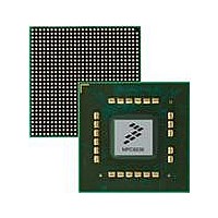
MPC8536DS Freescale Semiconductor, MPC8536DS Datasheet - Page 76

MPC8536DS
Manufacturer Part Number
MPC8536DS
Description
BOARD DEV SYSTEM MPC8536E
Manufacturer
Freescale Semiconductor
Series
PowerQUICC III™r
Type
MPUr
Datasheets
1.MPC8536EBVTAVLA.pdf
(127 pages)
2.MPC8536EBVTAVLA.pdf
(1706 pages)
3.MPC8536DS.pdf
(2 pages)
4.MPC8536DS.pdf
(126 pages)
Specifications of MPC8536DS
Contents
Board, Software and Documentation
Processor Series
MPC85xx
Core
e500
Data Bus Width
32 bit
Maximum Clock Frequency
667 MHz
Operating Supply Voltage
- 0.3 V to + 1.21 V
Maximum Operating Temperature
+ 105 C
Data Ram Size
32 KB
Interface Type
SPI, USB
Program Memory Type
DDR2, DDR3, SDRAM
Core Size
32 Bit
Program Memory Size
544KB
Cpu Speed
1.5GHz
Digital Ic Case Style
BGA
No. Of Pins
783
Supply Voltage Range
0.95V To 1.05V
Rohs Compliant
Yes
For Use With/related Products
MPC8536
Lead Free Status / RoHS Status
Lead free / RoHS Compliant
Enhanced Secure Digital Host Controller (eSDHC)
2.13.2
Table 56
76
At recommended operating conditions (see
At recommended operating conditions (see
SD_CLK clock frequency:
SD_CLK clock frequency - identification mode
SD_CLK clock low time - High speed/Full speed mode
SD_CLK clock high time - High speed/Full speed mode
SD_CLK clock rise and fall times
Input setup times: SD_CMD, SD_DATx, SD_CD to
SD_CLK
Input hold times: SD_CMD, SD_DATx, SD_CD to SD_CLK
Output delay time: SD_CLK to SD_CMD, SD_DATx valid
Notes:
1. The symbols used for timing specifications herein follow the pattern of t
2. In full speed mode, clock frequency value can be 0–25 MHz for a SD/SDIO card and 0–20 MHz for a MMC card. In high speed
3. 0 Hz means to stop the clock. The given minimum frequency range is for cases were a continuous clock is required.
4. To satisfy hold timing, the delay difference between clock input and cmd/data input must not exceed 2ns.
5. C
Output low voltage
Output high voltage
Output low voltage
Notes:
1. The min V
2. Open drain mode for MMC cards only.
for inputs and t
high speed mode device timing (SHS) clock reference (K) going to the high (H) state, with respect to the output (O) reaching
the invalid state (X) or output hold time. Note that, in general, the clock reference symbol representation is based on five letters
representing the clock of a particular functional. For rise and fall times, the latter convention is used with the appropriate letter:
R (rise) or F (fall).
mode, clock frequency value can be 0–50 MHz for a SD/SDIO card and 0–52MHz for a MMC card.
CARD
Characteristic
provides the eSDHC AC timing specifications as defined in
≤10 pF, (1 card), and C
eSDHC AC Timing Specifications
IL
and V
(first three letters of functional block)(reference)(state)(signal)(state)
SD/SDIO Full speed/high speed mode
MPC8536E PowerQUICC III Integrated Processor Hardware Specifications, Rev. 3
IH
Table 55. eSDHC interface DC Electrical Characteristics (continued)
MMC Full speed/high speed mode
Parameter
values are based on the respective min and max OV
L
Symbol
= C
V
V
V
OH
OL
OL
Table 56. eSDHC AC Timing Specifications
BUS
Table
Table
+ C
3)
3)
I
HOST
OL
= 100uA @OVDDmin
+C
I
OH
Condition
I
OL
CARD
= -100 uA
= 2 mA
≤ 40 pF
Symbol
t
t
t
t
t
t
t
SHSKHOV
SHSCKR/
SHSIVKH
SHSIXKH
f
SHSCKH
SHSCKF
SHSCKL
f
SHSCK
SIDCK
Figure
1
for outputs. For example, t
(first three letters of functional block)(signal)(state) (reference)(state)
OV
44.
IN
DD
Min
—
—
values found in
7/10
7/10
Min
100
- 0.2
2.5
–3
—
0
0
5
0.125 * OVDD
25/50
20/52
Max
Max
400
0.3
—
—
—
—
—
Table
3
3
FHSKHOV
Freescale Semiconductor
3.
symbolizes eSDHC
MHz
Unit
KHz
Unit
ns
ns
ns
ns
ns
ns
—
—
V
Notes
Notes
—
2, 5
3, 5
4,5
2
2
5
5
5
5
5


