HIP9011AB Intersil, HIP9011AB Datasheet
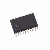
IC SENSOR ENGINE KNOCK 20-SOIC

HIP9011AB

Manufacturer Part Number
HIP9011AB
Description
IC SENSOR ENGINE KNOCK 20-SOIC
Manufacturer
Intersil
Type
Engine Knock Signal Processorr
Datasheet

Specifications of HIP9011AB

Input Type
Logic
Output Type
Logic
Interface
SPI
Current - Supply
8mA
Mounting Type
Surface Mount
Package / Case
20-SOIC (7.5mm Width)
Lead Free Status / RoHS Status
Contains lead / RoHS non-compliant

Available stocks

Company
Part Number
Manufacturer
Quantity
Price
Part Number:
HIP9011AB
Manufacturer:
INTERSIL
Quantity:
20 478
Part Number:
HIP9011AB
Manufacturer:
INTERSIL
Quantity:
19 565
Part Number:
HIP9011AB
Manufacturer:
INTERSIL
Quantity:
1 000
Part Number:
HIP9011AB
Manufacturer:
INTERSIL
Quantity:
20 000
Part Number:
HIP9011ABR4818
Manufacturer:
INTERSIL
Quantity:
7 306
Part Number:
HIP9011ABR7007
Manufacturer:
INTERSIL
Quantity:
6 665
Part Number:
HIP9011ABT
Manufacturer:
INTERSIL
Quantity:
20 000
Part Number:
HIP9011ABTS2457
Manufacturer:
PH
Quantity:
7 320
Part Number:
HIP9011ABZ
Manufacturer:
HAR
Quantity:
20 000
Part Number:
HIP9011ABZT
Manufacturer:
INTERSIL
Quantity:
20 000
Engine Knock Signal Processor
The HIP9011 is used to provide a method of detecting
premature detonation often referred to as “Knock or Ping” in
internal combustion engines.
The IC is shown in the Simplified Block Diagram. The chip
can select between one of two sensors, if needed for
accurate monitoring or for “V” type engines. Internal control
via the SPI bus is fast enough to switch sensors between
each firing cycle. A programmable bandpass filter
processes the signal from either of the sensor inputs. The
bandpass filter can be selected to optimize the extraction
the engine knock or ping signals from the engine
background noise. Further single processing is obtained by
full wave rectification of the filtered signal and applying it to
an integrator whose output voltage level is proportional to
the knock signal amplitude. The chip is under
microprocessor control via a SPI interface bus.
Ordering Information
Add “T” suffix for tape and reel.
NOTE: Intersil Pb-free plus anneal products employ special Pb-free
material sets; molding compounds/die attach materials and 100%
matte tin plate termination finish, which are RoHS compliant and
compatible with both SnPb and Pb-free soldering operations. Intersil
Pb-free products are MSL classified at Pb-free peak reflow
temperatures that meet or exceed the Pb-free requirements of
IPC/JEDEC J STD-020.
Simplified Block Diagram
HIP9011AB
HIP9011ABZ
(See Note)
NUMBER
PART
CH0FB
CH0IN
CH0NI
CH1FB
CH1IN
CH1NI
+
+
-
-
HIP9011AB
HIP9011ABZ
MARKING
PART
®
-40 to 125 20 Ld SOIC
RANGE
TEMP.
1
(
o
C)
VMID
Data Sheet
POWER SUPPLY
BIAS CIRCUITS
PROGRAMMABLE
(Pb-free)
2
V
PACKAGE
-
64 STEPS
DD
AND
STAGE
0.111
GAIN
GND
M20.3
M20.3
DWG. #
PKG.
1-888-INTERSIL or 1-888-468-3774
PROGRAMMABLE
CAUTION: These devices are sensitive to electrostatic discharge; follow proper IC Handling Procedures.
BANDPASS
64 STEPS
1
FILTER
-
20kHz
Features
• Two Sensor Inputs
• Microprocessor Programmable
• Accurate and Stable Filter Elements
• Digitally Programmable Gain
• Digitally Programmable Time Constants
• Digitally Programmable Filter Characteristics
• On-Chip Crystal Oscillator
• Programmable Frequency Divider
• External Clock Frequencies up to 24MHz
• Operating Temperature Range -40
• Pb-Free Plus Anneal Available (RoHS Compliant)
Applications
• Engine Knock Detector Processor
• Analog Signal Processing Where Controllable Filter
STATE MACHINE
- 4, 5, 6, 8, 10, 12, 16, 20, and 24MHz
Characteristics are Required
TEST
REGISTERS
TO SWITCHED
FULL WAVE
RECTIFIER
AND
NETWORKS
CAPACITOR
January 6, 2006
ACTIVE
All other trademarks mentioned are the property of their respective owners.
|
Intersil (and design) is a registered trademark of Intersil Americas Inc.
Copyright Intersil Americas Inc. 1999, 2006. All Rights Reserved
PROGRAMMABLE
PROGRAMMABLE
INTEGRATOR
40
32 STEPS
DIVIDER
-
600µs
INTERFACE
SPI
o
C to 125
AND HOLD
SAMPLE
OUTPUT
DRIVER
CLOCK
AND
HIP9011
o
FN4367.2
C
INT/HOLD
OSCOUT
INTOUT
OSCIN
SCK
SO
CS
SI

Related parts for HIP9011AB

HIP9011AB Summary of contents

Page 1

... C) HIP9011AB HIP9011AB -40 to 125 20 Ld SOIC HIP9011ABZ HIP9011ABZ -40 to 125 20 Ld SOIC (See Note) Add “T” suffix for tape and reel. NOTE: Intersil Pb-free plus anneal products employ special Pb-free material sets; molding compounds/die attach materials and 100% matte tin plate termination finish, which are RoHS compliant and compatible with both SnPb and Pb-free soldering operations ...

Page 2

Pinout Pin Descriptions PIN NUMBER DESIGNATION 1 V Five volt power input GND This pin is tied to ground This pin is connected to the internal mid-supply generator and is brought out for bypassing by a ...

Page 3

Absolute Maximum Ratings DC Logic Supply -0.5V to 7.0V DD Output Voltage ...

Page 4

GND = 0V, Clock Frequency 4MHz ±0.1%, T Electrical Specifications V DD Unless Otherwise Specified (Continued) PARAMETER INPUT AMPLIFIERS CH0 and CH1 High Output Voltage CH0 and CH1 Low Output Voltage Voltage Gain ANTIALIASING FILTER Response 1kHz ...

Page 5

Timing Diagrams INT/HOLD CS t CSCH SCK t CSCF SI t SUH SO SYMBOL t Minimum time from CS falling edge to SCK rising edge. CSCH t Minimum time from CS falling edge to SCK falling edge. CSCF t Minimum ...

Page 6

V DD VMID 0.022µF GND CH0NI CH1NI CH1IN R in CH1FB R F CH0IN R in CH0FB R F TRANSDUCERS OSCIN 20pF 4MHz OSCOUT 20pF 1MΩ FIGURE 3. SIMPLIFIED BLOCK DIAGRAM OF THE HIP9011 IN AN AUTOMOTIVE APPLICATION Description ...

Page 7

Circuit Block Description Input Amplifiers Two amplifiers can be selected to interface to the engine sensors. These amplifiers have a typical open loop gain of 100dB, with a typical bandwidth of 2.6MHz. The common mode input voltage range extends to ...

Page 8

Integration is enabled by the rising edge of the input control signal INT/HOLD. Within 20µs after the integrate input reaches a logic high level, the output of the integrator will fall to approximately V , 0.125V. The output of the ...

Page 9

TABLE 3. FREQUENCY, GAIN, AND INTEGRATOR TIME CONSTANT BIT VALUE PER FREQUENCY FUNCTION (kHz) 0 1.22 1 1.26 2 1.31 3 1.35 4 1.40 5 1.45 6 1.51 7 1.57 8 1.63 9 1.71 10 1.78 11 1.87 12 1.96 ...

Page 10

ADDRESS DECODER SI SCK CS FIGURE 5. PROGRAMMABLE REGISTERS AND STATE MACHINE The Digital SPI Block diagram in Figure 5 shows the programming flow of the chip. An eight bit word is received at the SI port. Data is shifted ...

Page 11

... Accordingly, the reader is cautioned to verify that data sheets are current before placing orders. Information furnished by Intersil is believed to be accurate and reliable. However, no responsibility is assumed by Intersil or its subsidiaries for its use; nor for any infringements of patents or other rights of third parties which may result from its use ...

Related keywords