IRF6612 International Rectifier, IRF6612 Datasheet

MOSFET N-CH 30V 24A DIRECTFET

IRF6612

Manufacturer Part Number
IRF6612
Description
MOSFET N-CH 30V 24A DIRECTFET
Manufacturer
International Rectifier
Series
HEXFET®r
Datasheet

Specifications of IRF6612

Fet Type
MOSFET N-Channel, Metal Oxide
Fet Feature
Logic Level Gate
Rds On (max) @ Id, Vgs
3.3 mOhm @ 24A, 10V
Drain To Source Voltage (vdss)
30V
Current - Continuous Drain (id) @ 25° C
24A
Vgs(th) (max) @ Id
2.25V @ 250µA
Gate Charge (qg) @ Vgs
45nC @ 4.5V
Input Capacitance (ciss) @ Vds
3970pF @ 15V
Power - Max
2.8W
Mounting Type
Surface Mount
Package / Case
DirectFET™ Isometric MX
Lead Free Status / RoHS Status
Contains lead / RoHS non-compliant
Other names
IRF6612TR

Available stocks

Company
Part Number
Manufacturer
Quantity
Price
Part Number:
IRF6612TRPBF
Manufacturer:
MAXIM
Quantity:
1 425
Part Number:
IRF6612TRPBF
Manufacturer:
IR
Quantity:
20 000
Company:
Part Number:
IRF6612TRPBF
Quantity:
1 838
l
l
l
l
l
l
l
l
www.irf.com
Applicable DirectFET Package/Layout Pad (see p.8,9 for details)
Description
The IRF6612 combines the latest HEXFET® power MOSFET silicon technology with the advanced DirectFET
ing to achieve the lowest on-state resistance in a package that has the footprint of a SO-8 and only 0.7 mm profile. The
DirectFET package is compatible with existing layout geometries used in power applications, PCB assembly equipment
and vapor phase, infra-red or convection soldering techniques, when application note AN-1035 is followed regarding the
manufacturing methods and processes. The DirectFET package allows dual sided cooling to maximize thermal transfer in
power systems, IMPROVING previous best thermal resistance by 80%.
The IRF6612 balances both low resistance and low charge along with ultra low package inductance to reduce both
conduction and switching losses. The reduced total losses make this product ideal for high efficiency DC-DC converters
that power the latest generation o f processors operating at higher frequencies. The IRF6612 has been optimized for
parameters that are critical in synchronous buck converters including R
immunity to minimize losses in the synchronous FET socket.
Absolute Maximum Ratings
V
V
I
I
I
I
P
P
P
T
T
Thermal Resistance
R
R
R
R
R
Notes  through
D
D
D
DM
J
STG
DS
GS
D
D
D
θJA
θJA
θJA
θJC
θJ-PCB
Techniques
RoHS compliant containing no lead or bromide
Application Specific MOSFETs
Ideal for CPU Core DC-DC Converters
Low Conduction Losses
Low Switching Losses
Low Profile (<0.7 mm)
Dual Sided Cooling Compatible
Compatible with Existing Surface Mount
@ T
@ T
@ T
@T
@T
@T
SQ
C
A
A
A
A
C
= 25°C
= 70°C
= 25°C
= 25°C
= 70°C
= 25°C
SX
Power Dissipation
Power Dissipation
Drain-to-Source Voltage
Gate-to-Source Voltage
Continuous Drain Current, V
Pulsed Drain Current
Power Dissipation
Linear Derating Factor
Operating Junction and
Storage Temperature Range
Junction-to-Ambient
Junction-to-Ambient
Junction-to-Ambient
Junction-to-Case
Junction-to-PCB Mounted
ˆ
ST
are on page 10
Parameter
Parameter
ij
g
g
fj
gj
hj
MQ
GS
GS
GS
@ 10V
@ 10V
@ 10V
IRF6612/IRF6612TR1
MX
V
30V
DSS
MT
DS(on)
Typ.
12.5
–––
–––
1.0
4.4mΩ@V
20
3.3mΩ@V
DirectFET™ Power MOSFET
, gate charge and Cdv/dt-induced turn on
R
-40 to + 150
DS(on)
Max.
0.022
136
190
±20
2.8
1.8
30
24
19
89
GS
GS
max
= 4.5V
= 10V
Max.
–––
–––
–––
1.4
45
DirectFET™ ISOMETRIC
Qg(typ.)
30nC
TM
Units
Units
W/°C
°C/W
°C
W
packag-
V
A
11/17/05
1

Related parts for IRF6612

IRF6612 Summary of contents

Page 1

... The reduced total losses make this product ideal for high efficiency DC-DC converters that power the latest generation o f processors operating at higher frequencies. The IRF6612 has been optimized for parameters that are critical in synchronous buck converters including R immunity to minimize losses in the synchronous FET socket ...

Page 2

Static @ T = 25°C (unless otherwise specified) J Parameter BV Drain-to-Source Breakdown Voltage DSS ∆ΒV /∆T Breakdown Voltage Temp. Coefficient DSS J R Static Drain-to-Source On-Resistance DS(on) V Gate Threshold Voltage GS(th) ∆V /∆T Gate Threshold Voltage Coefficient GS(th) ...

Page 3

VGS TOP 10V 7.0V 4.5V 4.0V 3.5V 1000 3.2V 2.9V BOTTOM 2.7V 100 10 2.7V ≤ 60µs PULSE WIDTH Tj = 25° Drain-to-Source Voltage (V) Typical Output Characteristics 1000 10V ...

Page 4

0V MHZ C iss = SHORTED C rss = oss = 10000 C iss C oss 1000 ...

Page 5

Case Temperature (°C) Maximum Drain Current vs. Case Temperature 100 D = 0.50 10 0.20 0.10 0.05 1 0.02 0.01 0.1 SINGLE PULSE 0.01 ( ...

Page 6

125° 25° GS, Gate -to -Source Voltage (V) On-Resistance vs. Gate Voltage 15V DRIVER ...

Page 7

D.U.T + ƒ • • - • + ‚ -  • • • SD • Vds Vgs(th) Qgs1 Qgs2 www.irf.com Driver Gate Drive P.W. D.U.T. I Waveform SD Reverse Recovery „ Current - + D.U.T. V Waveform DS Re-Applied ...

Page 8

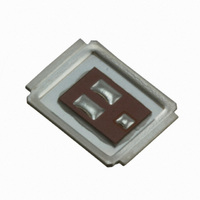
DIMENSIONS IMPERIAL METRIC CODE MIN MAX MIN MAX 6.35 0.246 A 6.25 0.250 5.05 0.189 B 4.80 0.201 3.95 0.152 C 3.85 0.156 0.45 0.014 D 0.35 0.018 0.72 E 0.68 0.027 0.028 0.72 0.027 F 0.68 0.028 ...

Page 9

D D www.irf.com G = GATE D = DRAIN S = SOURCE ...

Page 10

... NOTE: Controlling dimensions in mm Std reel quantity is 4800 parts. (ordered as IRF6612). For 1000 parts on 7" reel, order IRF6612TR1 STANDARD OPTION (QTY 4800) CODE MIN A 330.0 B 20.2 C 12.8 D 1.5 E 100.0 F N.C G 12.4 H 11.9 10 REEL DIMENSIONS TR1 OPTION (QTY 1000) METRIC IMPERIAL ...

Page 11

Notes:  ‚ Starting T = 25° 0.20mH 25Ω 19A ƒ Pulse width ≤ 400µs; duty cycle ≤ 2%. „ Surface mounted on 1 in. square Cu board. www.irf.com … ...

Page 12

Note: For the most current drawings please refer to the IR website at: http://www.irf.com/package/ ...

Related keywords