SD56120 STMicroelectronics, SD56120 Datasheet
SD56120
Specifications of SD56120
SD56120
Available stocks


Related parts for SD56120


SD56120 Summary of contents
Page 1
... The SD56120 is a common source N-Channel enhancement-mode lateral Field-Effect RF power transistor designed for broadband commercial and industrial applications at frequencies up to 1.0 GHz. The SD56120 is designed for high gain and broadband performance operating in common source mode ideal for broadcast applications from 470 to 860 MHz requiring high linearity ...
Page 2
... Contents Contents 1 Electrical data . . . . . . . . . . . . . . . . . . . . . . . . . . . . . . . . . . . . . . . . . . . . . . 3 1.1 Maximum ratings . . . . . . . . . . . . . . . . . . . . . . . . . . . . . . . . . . . . . . . . . . . . 3 1.2 Thermal data . . . . . . . . . . . . . . . . . . . . . . . . . . . . . . . . . . . . . . . . . . . . . . . 3 2 Electrical characteristics . . . . . . . . . . . . . . . . . . . . . . . . . . . . . . . . . . . . . 4 2.1 Static . . . . . . . . . . . . . . . . . . . . . . . . . . . . . . . . . . . . . . . . . . . . . . . . . . . . . 4 2.2 Dynamic . . . . . . . . . . . . . . . . . . . . . . . . . . . . . . . . . . . . . . . . . . . . . . . . . . . 4 3 Impedances . . . . . . . . . . . . . . . . . . . . . . . . . . . . . . . . . . . . . . . . . . . . . . . . 5 4 Typical performances . . . . . . . . . . . . . . . . . . . . . . . . . . . . . . . . . . . . . . . . 6 5 Test circuit . . . . . . . . . . . . . . . . . . . . . . . . . . . . . . . . . . . . . . . . . . . . . . . . . 9 6 Package mechanical data . . . . . . . . . . . . . . . . . . . . . . . . . . . . . . . . . . . . 12 7 Revision history . . . . . . . . . . . . . . . . . . . . . . . . . . . . . . . . . . . . . . . . . . . 14 2/15 Doc ID 6873 Rev 4 SD56120 ...
Page 3
... SD56120 1 Electrical data 1.1 Maximum ratings Table 2. Absolute maximum ratings (T Symbol V (BR)DSS DISS STG 1.2 Thermal data Table 3. Thermal data Symbol R thJC CASE Parameter Drain-source voltage Gate-source voltage Drain current Power dissipation (@ °C) Max. operating junction temperature Storage temperature Parameter Junction - case thermal resistance ...
Page 4
... MHz DQ = 400 100 860 MHz DQ OUT = 400 100 860 MHz DQ OUT = 400 100 W PEP DQ OUT = 400 100 860 MHz DQ OUT = 400 860 MHz DQ IN Doc ID 6873 Rev 4 SD56120 Min Typ Max Unit µA 1 µA 3.0 5.0 V 0.7 0 mho 2.8 pF ...
Page 5
... SD56120 3 Impedances Figure 2. Current conventions Table 6. Impedance data Freq. (MHz) 860 MHz Measured drain to drain and gate to gate respectively. Z (Ω 2.63 Doc ID 6873 Rev 4 Impedances Z (Ω 5.34 5/15 ...
Page 6
... Figure 4. VGS (NORMALIZED) 1. MHz per section 1. 0.98 0. -25 Figure 6. Pout (W) 140 120 100 Vds = 10 V per section Doc ID 6873 Rev 4 Gate-source voltage vs case temperature per section (°C) Output power vs input power Pin (W) SD56120 75 100 VDD = 28 V IDQ = 400 860 MHz 4 ...
Page 7
... SD56120 Figure 7. Power gain vs input power Pg (dB Pin (W) Figure 9. Power gain vs output power Gp (dB) 22 Idq = 800 mA 20 Idq = Idq = 400 mA 16 Idq = 600 mA Idq = 200 Pout (W) Figure 8. Nd (%) Vdd = Idq = 400 860 MHz Figure 10. Intermodulation distortion vs IMD3 (dBt -10 -15 -20 -25 -30 -35 ...
Page 8
... Figure 12. Output power vs bias current Pout (W) 120 115 110 105 Pin = 2.5 W Idq= 400 860 MHz 100 Vdd = 28 V Pin = 2 860 MHz 2 2.5 3 3.5 Doc ID 6873 Rev 4 Vdd = 28 V Pin = 2 860 MHz 0.2 0.4 0.6 0.8 1 1.2 1.4 1.6 Idq (A) SD56120 1.8 2 ...
Page 9
... SD56120 5 Test circuit Figure 14. 860 MHz test circuit schematic C16 Note: 1 Dimensions at component symbols are reference for component placement. 2 Gap between ground & transmission line = 0.056 [1.42] +0.002 [0.05] -0.000 [0.00] typ C28 C29 C31 C30 Doc ID 6873 Rev & Test circuit ...
Page 10
... Ohm 1/4 W carbon leaded resistor 82 Ohm 1/4 W carbon leaded resistor Balun, 50 Ohm Sucoform, OD 0.141 2.37 LG coaxial cable or equivalent Inductor, 6 Turn Air-wound #18AWG ID=0.130[3,30] magnet wire Surface-mount EMI shield bead Ultralam 2000. 0.030” thk εr = 2.55 both sides Doc ID 6873 Rev 4 SD56120 ...
Page 11
... SD56120 Figure 15. 860 MHz production test fixture Figure 16. 860 MHz test circuit photomaster + 6.4 inches Doc ID 6873 Rev 4 Test circuit + + 11/15 ...
Page 12
... Package mechanical data 6 Package mechanical data In order to meet environmental requirements, ST offers these devices in different grades of ® ECOPACK packages, depending on their level of environmental compliance. ECOPACK specifications, grade definitions and product status are available at: www.st.com. ® ECOPACK trademark. 12/15 Doc ID 6873 Rev 4 SD56120 ® ...
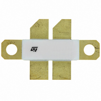
Page 13
... SD56120 Table 8. M246 (.230 x .650 WIDE 4/L BAL N/HERM W/FLG) mechanical data Dim Figure 17. Package dimensions Controlling dimension: Inches mm. Min Typ Max 5.33 5.59 6.48 6.73 17.27 18.29 5.72 5.97 22.86 28.83 29.08 16.26 16.76 4.19 5.08 0.08 0.15 1.83 2.24 1 ...
Page 14
... Revision history 7 Revision history Table 9. Document revision history Date 18-Jun-2001 12-Sep-2004 13-Jul-2006 02-Sep-2009 14/15 Revision 1 Initial release 2 Few updates 3 New template, added lead free info 4 Updated document’s title Doc ID 6873 Rev 4 SD56120 Changes ...
Page 15
... SD56120 Information in this document is provided solely in connection with ST products. STMicroelectronics NV and its subsidiaries (“ST”) reserve the right to make changes, corrections, modifications or improvements, to this document, and the products and services described herein at any time, without notice. All ST products are sold pursuant to ST’s terms and conditions of sale. ...