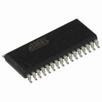
AT90PWM3B-16SU Atmel, AT90PWM3B-16SU Datasheet - Page 250

AT90PWM3B-16SU
Manufacturer Part Number
AT90PWM3B-16SU
Description
IC MCU AVR RISC 8K FLASH 32-SOIC
Manufacturer
Atmel
Series
AVR® 90PWM Lightingr
Specifications of AT90PWM3B-16SU
Core Processor
AVR
Core Size
8-Bit
Speed
16MHz
Connectivity
SPI, UART/USART
Peripherals
Brown-out Detect/Reset, POR, PWM, WDT
Number Of I /o
27
Program Memory Size
8KB (8K x 8)
Program Memory Type
FLASH
Eeprom Size
512 x 8
Ram Size
512 x 8
Voltage - Supply (vcc/vdd)
2.7 V ~ 5.5 V
Data Converters
A/D 11x10b; D/A 1x10b
Oscillator Type
Internal
Operating Temperature
-40°C ~ 105°C
Package / Case
32-SOIC (7.5mm Width)
Processor Series
AT90PWMx
Core
AVR8
Data Bus Width
8 bit
Data Ram Size
512 B
Interface Type
SPI/USART
Maximum Clock Frequency
16 MHz
Number Of Programmable I/os
27
Number Of Timers
2
Operating Supply Voltage
2.7 V to 5.5 V
Maximum Operating Temperature
+ 105 C
Mounting Style
SMD/SMT
3rd Party Development Tools
EWAVR, EWAVR-BL
Development Tools By Supplier
ATAVRDRAGON, ATSTK500, ATSTK600, ATAVRISP2, ATAVRONEKIT, ATAVRFBKIT, ATAVRISP2
Minimum Operating Temperature
- 40 C
On-chip Adc
11-ch x 10-bit
On-chip Dac
1-chx10-bit
Controller Family/series
AVR PWM
Eeprom Memory Size
512Byte
Ram Memory Size
512Byte
Cpu Speed
16MHz
Rohs Compliant
Yes
For Use With
ATSTK600-SOIC - STK600 SOCKET/ADAPTER FOR SOIC770-1007 - ISP 4PORT ATMEL AVR MCU SPI/JTAGATAVRMC200 - KIT EVAL FOR AT90PWM3 ASYNCATAVRFBKIT - KIT DEMO BALLAST FOR AT90PWM2ATAVRISP2 - PROGRAMMER AVR IN SYSTEMATSTK520 - ADAPTER KIT FOR 90PWM
Lead Free Status / RoHS Status
Lead free / RoHS Compliant
Available stocks
Company
Part Number
Manufacturer
Quantity
Price
Company:
Part Number:
AT90PWM3B-16SU
Manufacturer:
Atmel
Quantity:
4 000
Part Number:
AT90PWM3B-16SU
Manufacturer:
MICROCHIP/微芯
Quantity:
20 000
- Current page: 250 of 356
- Download datasheet (4Mb)
21.8.4.2
21.8.5
21.8.6
21.9
250
Amplifier
AT90PWM2/2B/3/3B
Digital Input Disable Register 0 – DIDR0
Digital Input Disable Register 1– DIDR1
ADLAR = 1
• Bit 7:0 – ADC7D..ADC0D: ACMP2:1 and ADC7:0 Digital Input Disable
When this bit is written logic one, the digital input buffer on the corresponding ADC pin is dis-
abled. The corresponding PIN Register bit will always read as zero when this bit is set. When an
analog signal is applied to the ADC7..0 pin and the digital input from this pin is not needed, this
bit should be written logic one to reduce power consumption in the digital input buffer.
• Bit 5:0 – ACMP0D, AMP0+D, AMP0-D, ADC10D..ADC8D: ACMP0, AMP1:0 and ADC10:8
When this bit is written logic one, the digital input buffer on the corresponding ADC pin is dis-
abled. The corresponding PIN Register bit will always read as zero when this bit is set. When an
analog signal is applied to an analog pin and the digital input from this pin is not needed, this bit
should be written logic one to reduce power consumption in the digital input buffer.
The AT90PWM2/2B/3/3B features two differential amplified channels with programmable 5, 10,
20, and 40 gain stage. Despite the result is given by the 10 bit ADC, the amplifier has been sized
to give a 8bits resolution.
Because the amplifier is a switching capacitor amplifier, it needs to be clocked by a synchroniza-
tion signal called in this document the amplifier synchronization clock. To ensure an accurate
result, the amplifier input needs to have a quite stable input value during at least 4 Amplifier syn-
chronization clock periods.
Amplified conversions can be synchronized to PSC events (See
Description in One/Two/Four Ramp Modes” on page 161
tion in Centered Mode” on page
clock frequency. In case the synchronization is done by the ADC clock divided by 8, this syn-
chronization is done automatically by the ADC interface in such a way that the sample-and-hold
occurs at a specific phase of CK
sions, and the first free running conversion) when CK
Bit
Read/Write
Initial Value
Bit
Read/Write
Initial Value
Bit
Read/Write
Initial Value
Digital Input Disable
ADC7D
ADC9
ADC1
R/W
7
R
R
0
0
7
0
7
0
-
-
ADC6D
ADC8
ADC0
R/W
6
0
6
0
R
R
6
0
0
-
-
ACMP0D
ADC2
ADC5D
ADC7
162) or to the internal clock CK
R/W
R/W
R
R
5
0
5
0
5
0
0
-
. A conversion initiated by the user (i.e., all single conver-
AMP0PD
ADC4D
ADC6
R/W
R/W
R
R
4
0
4
0
4
0
0
-
AMP0ND
ACMPM
ADC3D
ADC5
R/W
R/W
3
R
R
0
0
3
0
3
0
-
ADC2
and
ACMP2D
ACMP1D
ADC10D
is low will take the same amount of
ADC2D
ADC4
R/W
R/W
“Synchronization Source Descrip-
R
R
2
0
2
0
2
0
0
-
ADC
AMP1PD
ADC1D
ADC9D
“Synchronization Source
ADC3
R/W
R/W
equal to eighth the ADC
R
R
1
0
0
1
0
1
0
-
AMP1ND
ADC0D
ADC8D
ADC2
R/W
R/W
R
R
0
0
0
0
0
0
0
-
4317H–AVR–12/06
ADCH
ADCL
DIDR0
DIDR1
Related parts for AT90PWM3B-16SU
Image
Part Number
Description
Manufacturer
Datasheet
Request
R

Part Number:
Description:
Manufacturer:
Atmel Corporation
Datasheet:

Part Number:
Description:
IC MCU AVR RISC 8K FLASH 32-QFN
Manufacturer:
Atmel
Datasheet:

Part Number:
Description:
MCU AVR 8K FLASH 16MHA 32SOIC
Manufacturer:
Atmel
Datasheet:

Part Number:
Description:
IC AVR MCU FLASH 8K 32QFN
Manufacturer:
Atmel
Datasheet:

Part Number:
Description:
IC AVR MCU FLASH 8K 32SOIC
Manufacturer:
Atmel
Datasheet:

Part Number:
Description:
MCU AVR 8K FLASH 16MHZ 32-QFN
Manufacturer:
Atmel
Datasheet:

Part Number:
Description:
DEV KIT FOR AVR/AVR32
Manufacturer:
Atmel
Datasheet:

Part Number:
Description:
INTERVAL AND WIPE/WASH WIPER CONTROL IC WITH DELAY
Manufacturer:
ATMEL Corporation
Datasheet:

Part Number:
Description:
Low-Voltage Voice-Switched IC for Hands-Free Operation
Manufacturer:
ATMEL Corporation
Datasheet:

Part Number:
Description:
MONOLITHIC INTEGRATED FEATUREPHONE CIRCUIT
Manufacturer:
ATMEL Corporation
Datasheet:

Part Number:
Description:
AM-FM Receiver IC U4255BM-M
Manufacturer:
ATMEL Corporation
Datasheet:

Part Number:
Description:
Monolithic Integrated Feature Phone Circuit
Manufacturer:
ATMEL Corporation
Datasheet:

Part Number:
Description:
Multistandard Video-IF and Quasi Parallel Sound Processing
Manufacturer:
ATMEL Corporation
Datasheet:


