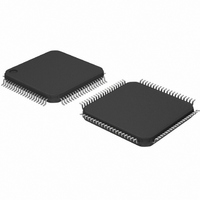
LPC1751FBD80,551 NXP Semiconductors, LPC1751FBD80,551 Datasheet - Page 11

LPC1751FBD80,551
Manufacturer Part Number
LPC1751FBD80,551
Description
IC ARM CORTEX MCU 32K 80-LQFP
Manufacturer
NXP Semiconductors
Series
LPC17xxr
Datasheet
1.LPC1751FBD80551.pdf
(74 pages)
Specifications of LPC1751FBD80,551
Program Memory Type
FLASH
Program Memory Size
32KB (32K x 8)
Package / Case
80-LQFP
Core Processor
ARM® Cortex-M3™
Core Size
32-Bit
Speed
100MHz
Connectivity
CAN, I²C, IrDA, Microwire, SPI, SSI, SSP, UART/USART, USB
Peripherals
Brown-out Detect/Reset, DMA, Motor Control PWM, POR, PWM, WDT
Number Of I /o
52
Ram Size
8K x 8
Voltage - Supply (vcc/vdd)
2.4 V ~ 3.6 V
Data Converters
A/D 6x12b
Oscillator Type
Internal
Operating Temperature
-40°C ~ 85°C
Processor Series
LPC17
Core
ARM Cortex M3
Data Bus Width
32 bit
Data Ram Size
8 KB
Interface Type
CAN, I2C, SPI, UART
Maximum Clock Frequency
100 MHz
Number Of Programmable I/os
52
Number Of Timers
3
Operating Supply Voltage
3.3 V
Maximum Operating Temperature
+ 85 C
Mounting Style
SMD/SMT
3rd Party Development Tools
MDK-ARM, RL-ARM, ULINK2
Minimum Operating Temperature
- 40 C
On-chip Adc
12 bit, 6 Channel
Cpu Family
LPC17xx
Device Core
ARM Cortex-M3
Device Core Size
32b
Frequency (max)
100MHz
Total Internal Ram Size
8KB
# I/os (max)
52
Number Of Timers - General Purpose
4
Operating Supply Voltage (typ)
3.3V
Operating Supply Voltage (max)
3.6V
Operating Supply Voltage (min)
2.4/2.7V
Instruction Set Architecture
RISC
Operating Temp Range
-40C to 85C
Operating Temperature Classification
Industrial
Mounting
Surface Mount
Pin Count
80
Package Type
LQFP
Package
80LQFP
Family Name
LPC17xx
Maximum Speed
100 MHz
Lead Free Status / RoHS Status
Lead free / RoHS Compliant
For Use With
622-1005 - USB IN-CIRCUIT PROG ARM7 LPC2K
Eeprom Size
-
Lead Free Status / Rohs Status
Lead free / RoHS Compliant
Other names
568-4788
935287916551
935287916551
Available stocks
Company
Part Number
Manufacturer
Quantity
Price
Company:
Part Number:
LPC1751FBD80,551
Manufacturer:
NXP Semiconductors
Quantity:
10 000
NXP Semiconductors
Table 3.
LPC1759_58_56_54_52_51
Product data sheet
Symbol
P2[8]/TD2/
TXD2
P2[9]/
USB_CONNECT/
RXD2
P2[10]/EINT0/NMI
P4[0] to P4[31]
P4[28]/RX_MCLK/
MAT2[0]/TXD3
P4[29]/TX_MCLK/
MAT2[1]/RXD3
TDO/SWO
TDI
TMS/SWDIO
TRST
TCK/SWDCLK
RSTOUT
RESET
XTAL1
XTAL2
RTCX1
RTCX2
V
SS
Pin description
Pin
50
49
41
65
68
1
2
3
4
5
11
14
19
20
13
15
24, 33,
43, 57,
66, 78
[6]
[7]
[7]
[7]
[6]
[1]
[1]
[5]
[1]
[1]
[8]
[9][10]
[9][10]
[9][11]
[9]
…continued
Type
I/O
O
O
I/O
O
I
I/O
I
I
I/O
I/O
I
O
O
I/O
I
O
I
O
O
I
I
I/O
I
I
I
O
I
I
O
I
O
I
Description
P2[8] — General purpose digital input/output pin.
TD2 — CAN2 transmitter output. (LPC1759/58/56 only).
TXD2 — Transmitter output for UART2.
P2[9] — General purpose digital input/output pin.
USB_CONNECT — Signal used to switch an external 1.5 kΩ resistor under
software control. Used with the SoftConnect USB feature.
RXD2 — Receiver input for UART2.
P2[10] — General purpose digital input/output pin. A LOW level on this pin during
reset starts the ISP command handler.
EINT0 — External interrupt 0 input.
NMI — Non-maskable interrupt input.
Port 4: Port 4 is a 32-bit I/O port with individual direction controls for each bit. The
operation of port 4 pins depends upon the pin function selected via the pin connect
block. Some port pins are not available on the LQFP80 package.
P4[28] — General purpose digital input/output pin.
RX_MCLK — I
MAT2[0] — Match output for Timer 2, channel 0.
TXD3 — Transmitter output for UART3.
P4[29] — General purpose digital input/output pin.
TX_MCLK — I
MAT2[1] — Match output for Timer 2, channel 1.
RXD3 — Receiver input for UART3.
TDO — Test Data out for JTAG interface.
SWO — Serial wire trace output.
TDI — Test Data in for JTAG interface.
TMS — Test Mode Select for JTAG interface.
SWDIO — Serial wire debug data input/output.
TRST — Test Reset for JTAG interface.
TCK — Test Clock for JTAG interface.
SWDCLK — Serial wire clock.
RSTOUT — This is a 3.3 V pin. LOW on this pin indicates
LPC1759/58/56/54/52/51 being in Reset state.
External reset input: A LOW on this pin resets the device, causing I/O ports and
peripherals to take on their default states, and processor execution to begin at
address 0. TTL with hysteresis, 5 V tolerant.
Input to the oscillator circuit and internal clock generator circuits.
Output from the oscillator amplifier.
Input to the RTC oscillator circuit.
Output from the RTC oscillator circuit.
ground: 0 V reference.
All information provided in this document is subject to legal disclaimers.
Rev. 6.01 — 11 March 2011
2
2
S transmit master clock. (LPC1759/58/56 only).
S receive master clock. (LPC1759/58/56 only).
LPC1759/58/56/54/52/51
32-bit ARM Cortex-M3 microcontroller
© NXP B.V. 2011. All rights reserved.
11 of 74


