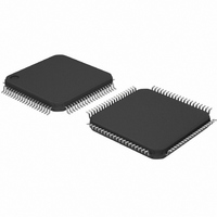
LPC1751FBD80,551 NXP Semiconductors, LPC1751FBD80,551 Datasheet - Page 66

LPC1751FBD80,551
Manufacturer Part Number
LPC1751FBD80,551
Description
IC ARM CORTEX MCU 32K 80-LQFP
Manufacturer
NXP Semiconductors
Series
LPC17xxr
Datasheet
1.LPC1751FBD80551.pdf
(74 pages)
Specifications of LPC1751FBD80,551
Program Memory Type
FLASH
Program Memory Size
32KB (32K x 8)
Package / Case
80-LQFP
Core Processor
ARM® Cortex-M3™
Core Size
32-Bit
Speed
100MHz
Connectivity
CAN, I²C, IrDA, Microwire, SPI, SSI, SSP, UART/USART, USB
Peripherals
Brown-out Detect/Reset, DMA, Motor Control PWM, POR, PWM, WDT
Number Of I /o
52
Ram Size
8K x 8
Voltage - Supply (vcc/vdd)
2.4 V ~ 3.6 V
Data Converters
A/D 6x12b
Oscillator Type
Internal
Operating Temperature
-40°C ~ 85°C
Processor Series
LPC17
Core
ARM Cortex M3
Data Bus Width
32 bit
Data Ram Size
8 KB
Interface Type
CAN, I2C, SPI, UART
Maximum Clock Frequency
100 MHz
Number Of Programmable I/os
52
Number Of Timers
3
Operating Supply Voltage
3.3 V
Maximum Operating Temperature
+ 85 C
Mounting Style
SMD/SMT
3rd Party Development Tools
MDK-ARM, RL-ARM, ULINK2
Minimum Operating Temperature
- 40 C
On-chip Adc
12 bit, 6 Channel
Cpu Family
LPC17xx
Device Core
ARM Cortex-M3
Device Core Size
32b
Frequency (max)
100MHz
Total Internal Ram Size
8KB
# I/os (max)
52
Number Of Timers - General Purpose
4
Operating Supply Voltage (typ)
3.3V
Operating Supply Voltage (max)
3.6V
Operating Supply Voltage (min)
2.4/2.7V
Instruction Set Architecture
RISC
Operating Temp Range
-40C to 85C
Operating Temperature Classification
Industrial
Mounting
Surface Mount
Pin Count
80
Package Type
LQFP
Package
80LQFP
Family Name
LPC17xx
Maximum Speed
100 MHz
Lead Free Status / RoHS Status
Lead free / RoHS Compliant
For Use With
622-1005 - USB IN-CIRCUIT PROG ARM7 LPC2K
Eeprom Size
-
Lead Free Status / Rohs Status
Lead free / RoHS Compliant
Other names
568-4788
935287916551
935287916551
Available stocks
Company
Part Number
Manufacturer
Quantity
Price
Company:
Part Number:
LPC1751FBD80,551
Manufacturer:
NXP Semiconductors
Quantity:
10 000
NXP Semiconductors
LPC1759_58_56_54_52_51
Product data sheet
14.4 Standard I/O pin configuration
order to keep the noise coupled in via the PCB as small as possible. Also parasitics
should stay as small as possible. Values of C
accordingly to the increase in parasitics of the PCB layout.
Figure 34
The default configuration for standard I/O pins is input with pull-up enabled. The weak
MOS devices provide a drive capability equivalent to pull-up and pull-down resistors.
Fig 34. Standard I/O pin configuration with analog input
•
•
•
•
•
as digital output
as analog input
as digital input
pin configured
pin configured
pin configured
Digital output driver: Open-drain mode enabled/disabled
Digital input: Pull-up enabled/disabled
Digital input: Pull-down enabled/disabled
Digital input: Repeater mode enabled/disabled
Analog input
driver
shows the possible pin modes for standard I/O pins with analog input function:
All information provided in this document is subject to legal disclaimers.
open-drain enable
repeater mode
output enable
analog input
Rev. 6.01 — 11 March 2011
data output
data input
enable
pull-down enable
LPC1759/58/56/54/52/51
pull-up enable
select analog input
x1
and C
32-bit ARM Cortex-M3 microcontroller
x2
should be chosen smaller
V
V
DD
DD
strong
pull-up
strong
pull-down
weak
pull-up
weak
pull-down
© NXP B.V. 2011. All rights reserved.
V
ESD
DD
ESD
V
SS
002aaf272
66 of 74
PIN


