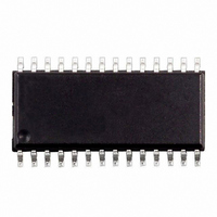
ST72F260G1M6 STMicroelectronics, ST72F260G1M6 Datasheet - Page 43

ST72F260G1M6
Manufacturer Part Number
ST72F260G1M6
Description
MCU 8BIT 4K FLASH ICP 28SOIC
Manufacturer
STMicroelectronics
Series
ST7r
Datasheet
1.STEVAL-ISQ002V1.pdf
(172 pages)
Specifications of ST72F260G1M6
Core Processor
ST7
Core Size
8-Bit
Speed
16MHz
Connectivity
SPI
Peripherals
LVD, POR, PWM, WDT
Number Of I /o
22
Program Memory Size
4KB (4K x 8)
Program Memory Type
FLASH
Ram Size
256 x 8
Voltage - Supply (vcc/vdd)
2.7 V ~ 5.5 V
Oscillator Type
Internal
Operating Temperature
-40°C ~ 85°C
Package / Case
28-SOIC (7.5mm Width)
Data Converters
A/D 6x10b
Processor Series
ST72F2x
Core
ST7
Data Bus Width
8 bit
Data Ram Size
256 B
Interface Type
I2C/SCI/SPI
Maximum Clock Frequency
8 MHz
Number Of Programmable I/os
22
Number Of Timers
3
Operating Supply Voltage
2.7 V to 5.5 V
Maximum Operating Temperature
+ 85 C
Mounting Style
SMD/SMT
Development Tools By Supplier
ST7F264-IND/USB, ST72F34X-SK/RAIS, ST7MDT10-DVP3, ST7MDT10-EMU3, STX-RLINK
Minimum Operating Temperature
- 40 C
On-chip Adc
6-ch x 10-bit
Controller Family/series
ST7
No. Of I/o's
22
Ram Memory Size
256Byte
Cpu Speed
8MHz
No. Of Timers
2
Embedded Interface Type
I2C, SCI, SPI
Rohs Compliant
Yes
For Use With
497-5046 - KIT TOOL FOR ST7/UPSD/STR7 MCU
Lead Free Status / RoHS Status
Lead free / RoHS Compliant
Eeprom Size
-
Lead Free Status / Rohs Status
Lead free / RoHS Compliant
Other names
497-4840
Available stocks
Company
Part Number
Manufacturer
Quantity
Price
I/O PORTS (Cont’d)
9.8 I/O PORT REGISTER DESCRIPTION
DATA REGISTER (DR)
Port x Data Register
PxDR with x = A, B or C.
Read/Write
Reset Value: 0000 0000 (00h)
Bits 7:0 = D[7:0] Data register 8 bits.
The DR register has a specific behaviour accord-
ing to the selected input/output configuration. Writ-
ing the DR register is always taken into account
even if the pin is configured as an input; this allows
always having the expected level on the pin when
toggling to output mode. Reading the DR register
returns either the DR register latch content (pin
configured as output) or the digital value applied to
the I/O pin (pin configured as input).
DATA DIRECTION REGISTER (DDR)
Port x Data Direction Register
PxDDR with x = A, B or C.
Read/Write
Reset Value: 0000 0000 (00h)
Bits 7:0 = DD[7:0] Data direction register 8 bits.
The DDR register gives the input/output direction
configuration of the pins. Each bit is set and
cleared by software.
0: Input mode
1: Output mode
DD7
D7
7
7
DD6
D6
DD5
D5
DD4
D4
DD3
D3
DD2
D2
DD1
D1
DD0
D0
0
0
OPTION REGISTER (OR)
Port x Option Register
PxOR with x = A, B or C.
Read/Write
Reset Value: 0000 0000 (00h)
Bits 7:0 = O[7:0] Option register 8 bits.
For specific I/O pins, this register is not implement-
ed. In this case the DDR register is enough to se-
lect the I/O pin configuration.
The OR register allows to distinguish: in input
mode if the pull-up with interrupt capability or the
basic pull-up configuration is selected, in output
mode if the push-pull or open drain configuration is
selected.
Each bit is set and cleared by software.
Input mode:
0: Floating input
1: Pull-up input with or without interrupt
Output mode:
0: Output open drain (with P-Buffer unactivated)
1: Output push-pull (when available)
O7
7
ST72260Gx, ST72262Gx, ST72264Gx
O6
O5
O4
O3
O2
O1
43/172
O0
0


