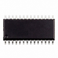
ST72F260G1M6 STMicroelectronics, ST72F260G1M6 Datasheet - Page 91

ST72F260G1M6
Manufacturer Part Number
ST72F260G1M6
Description
MCU 8BIT 4K FLASH ICP 28SOIC
Manufacturer
STMicroelectronics
Series
ST7r
Datasheet
1.STEVAL-ISQ002V1.pdf
(172 pages)
Specifications of ST72F260G1M6
Core Processor
ST7
Core Size
8-Bit
Speed
16MHz
Connectivity
SPI
Peripherals
LVD, POR, PWM, WDT
Number Of I /o
22
Program Memory Size
4KB (4K x 8)
Program Memory Type
FLASH
Ram Size
256 x 8
Voltage - Supply (vcc/vdd)
2.7 V ~ 5.5 V
Oscillator Type
Internal
Operating Temperature
-40°C ~ 85°C
Package / Case
28-SOIC (7.5mm Width)
Data Converters
A/D 6x10b
Processor Series
ST72F2x
Core
ST7
Data Bus Width
8 bit
Data Ram Size
256 B
Interface Type
I2C/SCI/SPI
Maximum Clock Frequency
8 MHz
Number Of Programmable I/os
22
Number Of Timers
3
Operating Supply Voltage
2.7 V to 5.5 V
Maximum Operating Temperature
+ 85 C
Mounting Style
SMD/SMT
Development Tools By Supplier
ST7F264-IND/USB, ST72F34X-SK/RAIS, ST7MDT10-DVP3, ST7MDT10-EMU3, STX-RLINK
Minimum Operating Temperature
- 40 C
On-chip Adc
6-ch x 10-bit
Controller Family/series
ST7
No. Of I/o's
22
Ram Memory Size
256Byte
Cpu Speed
8MHz
No. Of Timers
2
Embedded Interface Type
I2C, SCI, SPI
Rohs Compliant
Yes
For Use With
497-5046 - KIT TOOL FOR ST7/UPSD/STR7 MCU
Lead Free Status / RoHS Status
Lead free / RoHS Compliant
Eeprom Size
-
Lead Free Status / Rohs Status
Lead free / RoHS Compliant
Other names
497-4840
Available stocks
Company
Part Number
Manufacturer
Quantity
Price
SERIAL COMMUNICATIONS INTERFACE (Cont’d)
11.5.4.3 Receiver
The SCI can receive data words of either 8 or 9
bits. When the M bit is set, word length is 9 bits
and the MSB is stored in the R8 bit in the SCICR1
register.
Character reception
During a SCI reception, data shifts in least signifi-
cant bit first through the RDI pin. In this mode, the
SCIDR register consists or a buffer (RDR) be-
tween the internal bus and the received shift regis-
ter (see
Procedure
– Select the M bit to define the word length.
– Select the desired baud rate using the SCIBRR
– Set the RE bit, this enables the receiver which
When a character is received:
– The RDRF bit is set. It indicates that the content
– An interrupt is generated if the RIE bit is set and
– The error flags can be set if a frame error, noise
Clearing the RDRF bit is performed by the following
software sequence done by:
1. An access to the SCISR register
2. A read to the SCIDR register.
The RDRF bit must be cleared before the end of the
reception of the next character to avoid an overrun
error.
Break Character
When a break character is received, the SPI han-
dles it as a framing error.
Idle Character
When a idle frame is detected, there is the same
procedure as a data received character plus an in-
terrupt if the ILIE bit is set and the I bit is cleared in
the CCR register.
Overrun Error
An overrun error occurs when a character is re-
ceived when RDRF has not been reset. Data can
not be transferred from the shift register to the
and the SCIERPR registers.
begins searching for a start bit.
of the shift register is transferred to the RDR.
the I bit is cleared in the CCR register.
or an overrun error has been detected during re-
ception.
Figure
53).
RDR register as long as the RDRF bit is not
cleared.
When a overrun error occurs:
– The OR bit is set.
– The RDR content will not be lost.
– The shift register will be overwritten.
– An interrupt is generated if the RIE bit is set and
The OR bit is reset by an access to the SCISR reg-
ister followed by a SCIDR register read operation.
Noise Error
Oversampling techniques are used for data recov-
ery by discriminating between valid incoming data
and noise. Normal data bits are considered valid if
three consecutive samples (8th, 9th, 10th) have
the same bit value, otherwise the NF flag is set. In
the case of start bit detection, the NF flag is set on
the basis of an algorithm combining both valid
edge detection and three samples (8th, 9th, 10th).
Therefore, to prevent the NF flag getting set during
start bit reception, there should be a valid edge de-
tection as well as three valid samples.
When noise is detected in a frame:
– The NF flag is set at the rising edge of the RDRF
– Data is transferred from the Shift register to the
– No interrupt is generated. However this bit rises
The NF flag is reset by a SCISR register read op-
eration followed by a SCIDR register read opera-
tion.
During reception, if a false start bit is detected (e.g.
8th, 9th, 10th samples are 011,101,110), the
frame is discarded and the receiving sequence is
not started for this frame. There is no RDRF bit set
for this frame and the NF flag is set internally (not
accessible to the user). This NF flag is accessible
along with the RDRF bit when a next valid frame is
received.
Note: If the application Start Bit is not long enough
to match the above requirements, then the NF
Flag may get set due to the short Start Bit. In this
case, the NF flag may be ignored by the applica-
tion software when the first valid byte is received.
See also
the I bit is cleared in the CCR register.
bit.
SCIDR register.
at the same time as the RDRF bit which itself
generates an interrupt.
ST72260Gx, ST72262Gx, ST72264Gx
Section
11.5.4.10.
91/172


