MC68HC908JB8JPE Freescale Semiconductor, MC68HC908JB8JPE Datasheet - Page 134
MC68HC908JB8JPE
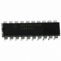
Manufacturer Part Number
MC68HC908JB8JPE
Description
IC MCU FLASH 8BIT 8K 20-DIP
Manufacturer
Freescale Semiconductor
Series
HC08r
Datasheet
1.MC908JB8JDWE.pdf
(286 pages)
Specifications of MC68HC908JB8JPE
Core Processor
HC08
Core Size
8-Bit
Speed
3MHz
Connectivity
USB
Peripherals
LVD, POR, PWM
Number Of I /o
13
Program Memory Size
8KB (8K x 8)
Program Memory Type
FLASH
Ram Size
256 x 8
Voltage - Supply (vcc/vdd)
4 V ~ 5.5 V
Oscillator Type
Internal
Operating Temperature
0°C ~ 70°C
Package / Case
20-DIP (0.300", 7.62mm)
Controller Family/series
HC08
No. Of I/o's
13
Ram Memory Size
256Byte
Cpu Speed
3MHz
No. Of Timers
1
Embedded Interface Type
USB
Rohs Compliant
Yes
Processor Series
HC08JB
Core
HC08
Data Bus Width
8 bit
Data Ram Size
256 B
Interface Type
USB
Maximum Clock Frequency
3 MHz
Number Of Programmable I/os
37
Number Of Timers
2
Operating Supply Voltage
4 V to 5.5 V
Maximum Operating Temperature
+ 70 C
Mounting Style
Through Hole
Development Tools By Supplier
FSICEBASE, DEMO908GZ60E, M68EML08GZE, KITUSBSPIDGLEVME, KITUSBSPIEVME, KIT33810EKEVME
Minimum Operating Temperature
0 C
Lead Free Status / RoHS Status
Lead free / RoHS Compliant
Eeprom Size
-
Data Converters
-
Lead Free Status / Rohs Status
Details


Universal Serial Bus Module (USB)
9.7.2.1 Output Driver Characteristics
9.7.2.2 Low Speed (1.5 Mbps) Driver Characteristics
Technical Data
134
The USB transceiver uses a differential output driver to drive the USB
data signal onto the USB cable. The static output swing of the driver in
its low state is below the V
its high state is above the V
output swings between the differential high and low state are well
balanced to minimize signal skew. Slew rate control on the driver is used
to minimize the radiated noise and cross talk. The driver’s outputs
support 3-state operation to achieve bidirectional half duplex operation.
The driver can tolerate a voltage on the signal pins of –1.0V to 5.5V with
respect to local ground reference without damage.
The rise and fall time of the signals on this cable are greater than 75ns
and less than 300ns. The edges are matched to within
RFI emissions and signal skew.
USB data transmission is done with differential signals. A differential
input receiver is used to accept the USB data signal. A differential 1 on
the bus is represented by D+ being at least 200mV more positive than
D– as seen at the receiver, and a differential 0 is represented by D–
being at least 200mV more positive than D+ as seen at the receiver. The
signal cross over point must be between 1.3V and 2.0V.
V
V
SE
SE
(max)
(min.)
V
SS
Universal Serial Bus Module (USB)
Figure 9-11. Receiver Characteristics
(1.5 Mb/s)
ONE BIT
TIME
MC68HC908JB8•MC68HC08JB8•MC68HC08JT8 — Rev. 2.3
OL
OH
of 0.3V with a 1.5kΩ load to 3.6V and in
of 2.8V with a 15kΩ load to ground. The
REFLECTIONS AND RINGING
LEVELS WITH MINIMAL
PASS OUTPUT SPEC
SIGNAL PINS
Freescale Semiconductor
±
20% to minimize
Related parts for MC68HC908JB8JPE
Image
Part Number
Description
Manufacturer
Datasheet
Request
R

Part Number:
Description:
Manufacturer:
Freescale Semiconductor, Inc
Datasheet:
Part Number:
Description:
Manufacturer:
Freescale Semiconductor, Inc
Datasheet:
Part Number:
Description:
Manufacturer:
Freescale Semiconductor, Inc
Datasheet:
Part Number:
Description:
Manufacturer:
Freescale Semiconductor, Inc
Datasheet:
Part Number:
Description:
Manufacturer:
Freescale Semiconductor, Inc
Datasheet:
Part Number:
Description:
Manufacturer:
Freescale Semiconductor, Inc
Datasheet:
Part Number:
Description:
Manufacturer:
Freescale Semiconductor, Inc
Datasheet:
Part Number:
Description:
Manufacturer:
Freescale Semiconductor, Inc
Datasheet:
Part Number:
Description:
Manufacturer:
Freescale Semiconductor, Inc
Datasheet:
Part Number:
Description:
Manufacturer:
Freescale Semiconductor, Inc
Datasheet:
Part Number:
Description:
Manufacturer:
Freescale Semiconductor, Inc
Datasheet:
Part Number:
Description:
Manufacturer:
Freescale Semiconductor, Inc
Datasheet:
Part Number:
Description:
Manufacturer:
Freescale Semiconductor, Inc
Datasheet:
Part Number:
Description:
Manufacturer:
Freescale Semiconductor, Inc
Datasheet:
Part Number:
Description:
Manufacturer:
Freescale Semiconductor, Inc
Datasheet: