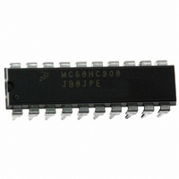
MC68HC908JB8JPE Freescale Semiconductor, MC68HC908JB8JPE Datasheet - Page 243

MC68HC908JB8JPE
Manufacturer Part Number
MC68HC908JB8JPE
Description
IC MCU FLASH 8BIT 8K 20-DIP
Manufacturer
Freescale Semiconductor
Series
HC08r
Datasheet
1.MC908JB8JDWE.pdf
(286 pages)
Specifications of MC68HC908JB8JPE
Core Processor
HC08
Core Size
8-Bit
Speed
3MHz
Connectivity
USB
Peripherals
LVD, POR, PWM
Number Of I /o
13
Program Memory Size
8KB (8K x 8)
Program Memory Type
FLASH
Ram Size
256 x 8
Voltage - Supply (vcc/vdd)
4 V ~ 5.5 V
Oscillator Type
Internal
Operating Temperature
0°C ~ 70°C
Package / Case
20-DIP (0.300", 7.62mm)
Controller Family/series
HC08
No. Of I/o's
13
Ram Memory Size
256Byte
Cpu Speed
3MHz
No. Of Timers
1
Embedded Interface Type
USB
Rohs Compliant
Yes
Processor Series
HC08JB
Core
HC08
Data Bus Width
8 bit
Data Ram Size
256 B
Interface Type
USB
Maximum Clock Frequency
3 MHz
Number Of Programmable I/os
37
Number Of Timers
2
Operating Supply Voltage
4 V to 5.5 V
Maximum Operating Temperature
+ 70 C
Mounting Style
Through Hole
Development Tools By Supplier
FSICEBASE, DEMO908GZ60E, M68EML08GZE, KITUSBSPIDGLEVME, KITUSBSPIEVME, KIT33810EKEVME
Minimum Operating Temperature
0 C
Lead Free Status / RoHS Status
Lead free / RoHS Compliant
Eeprom Size
-
Data Converters
-
Lead Free Status / Rohs Status
Details
- Current page: 243 of 286
- Download datasheet (2Mb)
Technical Data — MC68HC908JB8•MC68HC08JB8•MC68HC08JT8
16.1 Contents
16.2 Introduction
16.3 Functional Description
MC68HC908JB8•MC68HC08JB8•MC68HC08JT8 — Rev. 2.3
Freescale Semiconductor
16.2
16.3
16.4
16.5
16.5.1
16.5.2
This section describes the low-voltage inhibit module (LVI), which
monitors the voltage on the V
voltage falls to the LVI trip (V
Figure 16-1
after a reset. The LVI module contains a bandgap reference circuit and
comparator. Setting LVI disable bit (LVID) disables the LVI to monitor
V
The LVI module generates one output signal:
LVI Reset — an reset signal will be generated to reset the CPU when
V
DD
DD
voltage.
drops to below the set trip point.
Introduction . . . . . . . . . . . . . . . . . . . . . . . . . . . . . . . . . . . . . . . 243
Low-Power Modes . . . . . . . . . . . . . . . . . . . . . . . . . . . . . . . . . 244
Functional Description . . . . . . . . . . . . . . . . . . . . . . . . . . . . . .243
LVI Control Register (CONFIG) . . . . . . . . . . . . . . . . . . . . . . .244
Wait Mode . . . . . . . . . . . . . . . . . . . . . . . . . . . . . . . . . . . . .244
Stop Mode . . . . . . . . . . . . . . . . . . . . . . . . . . . . . . . . . . . . .244
Section 16. Low Voltage Inhibit (LVI)
shows the structure of the LVI module. The LVI is enabled
Low Voltage Inhibit (LVI)
DD
LVR
pin and generates a reset when the V
) voltage.
Technical Data
243
DD
Related parts for MC68HC908JB8JPE
Image
Part Number
Description
Manufacturer
Datasheet
Request
R
Part Number:
Description:
Manufacturer:
Freescale Semiconductor, Inc
Datasheet:
Part Number:
Description:
Manufacturer:
Freescale Semiconductor, Inc
Datasheet:
Part Number:
Description:
Manufacturer:
Freescale Semiconductor, Inc
Datasheet:
Part Number:
Description:
Manufacturer:
Freescale Semiconductor, Inc
Datasheet:
Part Number:
Description:
Manufacturer:
Freescale Semiconductor, Inc
Datasheet:
Part Number:
Description:
Manufacturer:
Freescale Semiconductor, Inc
Datasheet:
Part Number:
Description:
Manufacturer:
Freescale Semiconductor, Inc
Datasheet:
Part Number:
Description:
Manufacturer:
Freescale Semiconductor, Inc
Datasheet:
Part Number:
Description:
Manufacturer:
Freescale Semiconductor, Inc
Datasheet:
Part Number:
Description:
Manufacturer:
Freescale Semiconductor, Inc
Datasheet:
Part Number:
Description:
Manufacturer:
Freescale Semiconductor, Inc
Datasheet:
Part Number:
Description:
Manufacturer:
Freescale Semiconductor, Inc
Datasheet:
Part Number:
Description:
Manufacturer:
Freescale Semiconductor, Inc
Datasheet:
Part Number:
Description:
Manufacturer:
Freescale Semiconductor, Inc
Datasheet:
Part Number:
Description:
Manufacturer:
Freescale Semiconductor, Inc
Datasheet:


