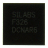
C8051F326-GM Silicon Laboratories Inc, C8051F326-GM Datasheet - Page 123

C8051F326-GM
Manufacturer Part Number
C8051F326-GM
Description
IC 8051 MCU FLASH 16K 28QFN
Manufacturer
Silicon Laboratories Inc
Series
C8051F32xr
Specifications of C8051F326-GM
Program Memory Type
FLASH
Program Memory Size
16KB (16K x 8)
Package / Case
28-QFN
Core Processor
8051
Core Size
8-Bit
Speed
25MHz
Connectivity
UART/USART, USB
Peripherals
POR
Number Of I /o
15
Ram Size
1.5K x 8
Voltage - Supply (vcc/vdd)
2.7 V ~ 3.6 V
Oscillator Type
Internal
Operating Temperature
-40°C ~ 85°C
Processor Series
C8051F3x
Core
8051
Data Bus Width
8 bit
Data Ram Size
1.5 KB
Interface Type
UART/USB
Maximum Clock Frequency
25 MHz
Number Of Programmable I/os
15
Number Of Timers
2
Operating Supply Voltage
2.7 V to 3.6 V
Maximum Operating Temperature
+ 85 C
Mounting Style
SMD/SMT
3rd Party Development Tools
PK51, CA51, A51, ULINK2
Development Tools By Supplier
C8051F320DK
Minimum Operating Temperature
- 40 C
No. Of I/o's
15
Ram Memory Size
1280Byte
Cpu Speed
25MHz
No. Of Timers
2
Digital Ic Case Style
QFN
Supply Voltage
RoHS Compliant
Package
28QFN EP
Device Core
8051
Family Name
C8051F326
Maximum Speed
25 MHz
Lead Free Status / RoHS Status
Lead free / RoHS Compliant
For Use With
770-1006 - ISP 4PORT FOR SILABS C8051F MCU336-1450 - ADAPTER PROGRAM TOOLSTICK F326336-1306 - KIT DEV FOR C8051F326/7
Eeprom Size
-
Data Converters
-
Lead Free Status / Rohs Status
Lead free / RoHS Compliant
Other names
336-1296-5
Available stocks
Company
Part Number
Manufacturer
Quantity
Price
Company:
Part Number:
C8051F326-GM
Manufacturer:
SiliconL
Quantity:
811
Part Number:
C8051F326-GMR
Manufacturer:
SILICON LABS/芯科
Quantity:
20 000
Bit7:
Bit6:
Bit5:
Bit4:
Bit3:
Bit2:
Bit1:
Bit0:
OVR0
R/W
Bit7
OVR0: Receive FIFO Overrun Flag.
This bit is used to indicate a receive FIFO overrun condition.
0: Receive FIFO Overrun has not occurred.
1: Receive FIFO Overrun has occurred (an incoming character was discarded due to a full
FIFO).
This bit must be cleared to ‘0’ by software.
PERR0: Parity Error Flag.
When parity is enabled, this bit is used to indicate that a parity error has occurred. It is set to
‘1’ when the parity of the oldest byte in the FIFO does not match the selected Parity Type.
0: Parity Error has not occurred.
1: Parity Error has occurred.
This bit must be cleared to ‘0’ by software.
Unused. Read = 1b. Write = don’t care.
REN0: Receive Enable.
This bit enables/disables the UART receiver. When disabled, bytes can still be read from the
receive FIFO.
0: UART0 reception disabled.
1: UART0 reception enabled.
TBX0: Extra Transmission Bit.
The logic level of this bit will be assigned to the extra transmission bit when XBE0 is set to
‘1’. This bit is not used when Parity is enabled.
RBX0: Extra Receive Bit.
RBX0 is assigned the value of the extra bit when XBE0 is set to ‘1’. If XBE0 is cleared to ‘0’,
RBX0 will be assigned the logic level of the first stop bit. This bit is not valid when Parity is
enabled.
TI0: Transmit Interrupt Flag.
Set to a ‘1’ by hardware after data has been transmitted, at the beginning of the STOP bit.
When the UART0 interrupt is enabled, setting this bit causes the CPU to vector to the
UART0 interrupt service routine. This bit must be cleared manually by software.
RI0: Receive Interrupt Flag.
Set to ‘1’ by hardware when a byte of data has been received by UART0 (set at the STOP bit
sampling time). When the UART0 interrupt is enabled, setting this bit to ‘1’ causes the CPU
to vector to the UART0 interrupt service routine. This bit must be cleared manually by soft-
ware.
PERR0
R/W
Bit6
SFR Definition 13.1. SCON0: UART0 Control
Bit5
—
R
REN0
R/W
Bit4
Rev. 1.1
TBX0
R/W
Bit3
RBX0
R/W
Bit2
R/W
TI0
Bit1
C8051F326/7
SFR Address:
R/W
RI0
Bit0
0x98
00100000
Addressable
Reset Value
Bit
123


