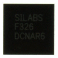
C8051F326-GM Silicon Laboratories Inc, C8051F326-GM Datasheet - Page 25

C8051F326-GM
Manufacturer Part Number
C8051F326-GM
Description
IC 8051 MCU FLASH 16K 28QFN
Manufacturer
Silicon Laboratories Inc
Series
C8051F32xr
Specifications of C8051F326-GM
Program Memory Type
FLASH
Program Memory Size
16KB (16K x 8)
Package / Case
28-QFN
Core Processor
8051
Core Size
8-Bit
Speed
25MHz
Connectivity
UART/USART, USB
Peripherals
POR
Number Of I /o
15
Ram Size
1.5K x 8
Voltage - Supply (vcc/vdd)
2.7 V ~ 3.6 V
Oscillator Type
Internal
Operating Temperature
-40°C ~ 85°C
Processor Series
C8051F3x
Core
8051
Data Bus Width
8 bit
Data Ram Size
1.5 KB
Interface Type
UART/USB
Maximum Clock Frequency
25 MHz
Number Of Programmable I/os
15
Number Of Timers
2
Operating Supply Voltage
2.7 V to 3.6 V
Maximum Operating Temperature
+ 85 C
Mounting Style
SMD/SMT
3rd Party Development Tools
PK51, CA51, A51, ULINK2
Development Tools By Supplier
C8051F320DK
Minimum Operating Temperature
- 40 C
No. Of I/o's
15
Ram Memory Size
1280Byte
Cpu Speed
25MHz
No. Of Timers
2
Digital Ic Case Style
QFN
Supply Voltage
RoHS Compliant
Package
28QFN EP
Device Core
8051
Family Name
C8051F326
Maximum Speed
25 MHz
Lead Free Status / RoHS Status
Lead free / RoHS Compliant
For Use With
770-1006 - ISP 4PORT FOR SILABS C8051F MCU336-1450 - ADAPTER PROGRAM TOOLSTICK F326336-1306 - KIT DEV FOR C8051F326/7
Eeprom Size
-
Data Converters
-
Lead Free Status / Rohs Status
Lead free / RoHS Compliant
Other names
336-1296-5
Available stocks
Company
Part Number
Manufacturer
Quantity
Price
Company:
Part Number:
C8051F326-GM
Manufacturer:
SiliconL
Quantity:
811
Part Number:
C8051F326-GMR
Manufacturer:
SILICON LABS/芯科
Quantity:
20 000
4.
REGIN
XTAL2
Pinout and Package Definitions
Name
VBUS
C2CK
P3.0/
P0.3/
GND
RST/
VDD
P0.0
P0.1
P0.2
P0.4
P0.5
C2D
VIO
D+
D–
Pin Numbers
‘F326
10
28
27
26
25
24
6
5
2
9
7
8
3
4
1
Table 4.1. Pin Definitions for the C8051F326/7
‘F327
—
10
28
27
26
25
6
3
9
7
8
4
5
2
1
Power
Power
Power
Power
D I/O
D I/O
D I/O
D I/O
D I/O
D I/O
D I/O
D I/O
D I/O
D I/O
D I/O
D I/O
Type
D In
D In
Out
In
In
In
Description
2.7–3.6 V Core Supply Voltage Input.
3.3 V Voltage Regulator Output. See Section 5.
V I/O Supply Voltage Input. The voltage at this pin must be
less than or equal to the Core Supply Voltage (V
'F326. On the 'F327, this pin is internally connected to V
Ground.
Device Reset. Open-drain output of internal POR or VDD
monitor. An external source can initiate a system reset by
driving this pin low for at least 15 µs. See Section 7.
Clock signal for the C2 Debug Interface.
Port 3.0. See Section 11 for a complete description.
Bi-directional data signal for the C2 Debug Interface.
5 V Regulator Input. This pin is the input to the on-chip volt-
age regulator.
VBUS Sense Input. This pin should be connected to the
VBUS signal of a USB network. A 5 V signal on this pin indi-
cates a USB network connection.
USB D+.
USB D–.
Port 0.0. See Section 11 for a complete description.
Port 0.1. See Section 11 for a complete description.
Port 0.2. See Section 11 for a complete description.
Port 0.3. See Section 11 for a complete description.
External Clock Input. See Section 10 for a complete
description.
Port 0.4. See Section 11 for a complete description.
Port 0.5. See Section 11 for a complete description.
Rev. 1.1
C8051F326/7
DD
) for the
DD
25
.


