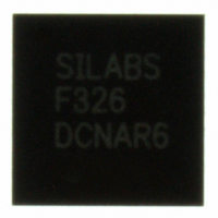
C8051F326-GM Silicon Laboratories Inc, C8051F326-GM Datasheet - Page 46

C8051F326-GM
Manufacturer Part Number
C8051F326-GM
Description
IC 8051 MCU FLASH 16K 28QFN
Manufacturer
Silicon Laboratories Inc
Series
C8051F32xr
Specifications of C8051F326-GM
Program Memory Type
FLASH
Program Memory Size
16KB (16K x 8)
Package / Case
28-QFN
Core Processor
8051
Core Size
8-Bit
Speed
25MHz
Connectivity
UART/USART, USB
Peripherals
POR
Number Of I /o
15
Ram Size
1.5K x 8
Voltage - Supply (vcc/vdd)
2.7 V ~ 3.6 V
Oscillator Type
Internal
Operating Temperature
-40°C ~ 85°C
Processor Series
C8051F3x
Core
8051
Data Bus Width
8 bit
Data Ram Size
1.5 KB
Interface Type
UART/USB
Maximum Clock Frequency
25 MHz
Number Of Programmable I/os
15
Number Of Timers
2
Operating Supply Voltage
2.7 V to 3.6 V
Maximum Operating Temperature
+ 85 C
Mounting Style
SMD/SMT
3rd Party Development Tools
PK51, CA51, A51, ULINK2
Development Tools By Supplier
C8051F320DK
Minimum Operating Temperature
- 40 C
No. Of I/o's
15
Ram Memory Size
1280Byte
Cpu Speed
25MHz
No. Of Timers
2
Digital Ic Case Style
QFN
Supply Voltage
RoHS Compliant
Package
28QFN EP
Device Core
8051
Family Name
C8051F326
Maximum Speed
25 MHz
Lead Free Status / RoHS Status
Lead free / RoHS Compliant
For Use With
770-1006 - ISP 4PORT FOR SILABS C8051F MCU336-1450 - ADAPTER PROGRAM TOOLSTICK F326336-1306 - KIT DEV FOR C8051F326/7
Eeprom Size
-
Data Converters
-
Lead Free Status / Rohs Status
Lead free / RoHS Compliant
Other names
336-1296-5
Available stocks
Company
Part Number
Manufacturer
Quantity
Price
Company:
Part Number:
C8051F326-GM
Manufacturer:
SiliconL
Quantity:
811
Part Number:
C8051F326-GMR
Manufacturer:
SILICON LABS/芯科
Quantity:
20 000
C8051F326/7
46
Bit7:
Bit6:
Bit5:
Bits4–3: RS1-RS0: Register Bank Select.
Bit2:
Bit1:
Bit0:
Bits7–0: ACC: Accumulator.
ACC.7
R/W
R/W
CY
Bit7
Bit7
CY: Carry Flag.
This bit is set when the last arithmetic operation resulted in a carry (addition) or a borrow
(subtraction). It is cleared to logic 0 by all other arithmetic operations.
AC: Auxiliary Carry Flag
This bit is set when the last arithmetic operation resulted in a carry into (addition) or a borrow
from (subtraction) the high order nibble. It is cleared to logic 0 by all other arithmetic opera-
tions.
F0: User Flag 0.
This is a bit-addressable, general purpose flag for use under software control.
These bits select which register bank is used during register accesses.
OV: Overflow Flag.
This bit is set to 1 under the following circumstances:
• An ADD, ADDC, or SUBB instruction causes a sign-change overflow.
• A MUL instruction results in an overflow (result is greater than 255).
• A DIV instruction causes a divide-by-zero condition.
The OV bit is cleared to 0 by the ADD, ADDC, SUBB, MUL, and DIV instructions in all other
cases.
F1: User Flag 1.
This is a bit-addressable, general purpose flag for use under software control.
PARITY: Parity Flag.
This register is the accumulator for arithmetic operations.
RS1
ACC.6
0
0
1
1
R/W
R/W
AC
Bit6
Bit6
SFR Definition 6.4. PSW: Program Status Word
RS0
0
1
0
1
ACC.5
R/W
SFR Definition 6.5. ACC: Accumulator
R/W
Bit5
Bit5
F0
Register Bank
ACC.4
RS1
R/W
R/W
Bit4
Bit4
0
1
2
3
Rev. 1.1
ACC.3
RS0
R/W
R/W
Bit3
Bit3
0x00–0x07
0x08–0x0F
0x10–0x17
0x18–0x1F
Address
ACC.2
R/W
R/W
OV
Bit2
Bit2
ACC.1
R/W
R/W
Bit1
Bit1
F1
(bit addressable)
(bit addressable)
PARITY
ACC.0
R/W
Bit0
Bit0
R
SFR Address:
SFR Address:
00000000
00000000
Reset Value
Reset Value
0xD0
0xE0


