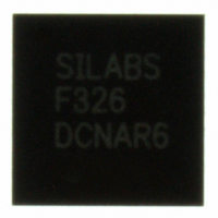
C8051F326-GM Silicon Laboratories Inc, C8051F326-GM Datasheet - Page 95

C8051F326-GM
Manufacturer Part Number
C8051F326-GM
Description
IC 8051 MCU FLASH 16K 28QFN
Manufacturer
Silicon Laboratories Inc
Series
C8051F32xr
Specifications of C8051F326-GM
Program Memory Type
FLASH
Program Memory Size
16KB (16K x 8)
Package / Case
28-QFN
Core Processor
8051
Core Size
8-Bit
Speed
25MHz
Connectivity
UART/USART, USB
Peripherals
POR
Number Of I /o
15
Ram Size
1.5K x 8
Voltage - Supply (vcc/vdd)
2.7 V ~ 3.6 V
Oscillator Type
Internal
Operating Temperature
-40°C ~ 85°C
Processor Series
C8051F3x
Core
8051
Data Bus Width
8 bit
Data Ram Size
1.5 KB
Interface Type
UART/USB
Maximum Clock Frequency
25 MHz
Number Of Programmable I/os
15
Number Of Timers
2
Operating Supply Voltage
2.7 V to 3.6 V
Maximum Operating Temperature
+ 85 C
Mounting Style
SMD/SMT
3rd Party Development Tools
PK51, CA51, A51, ULINK2
Development Tools By Supplier
C8051F320DK
Minimum Operating Temperature
- 40 C
No. Of I/o's
15
Ram Memory Size
1280Byte
Cpu Speed
25MHz
No. Of Timers
2
Digital Ic Case Style
QFN
Supply Voltage
RoHS Compliant
Package
28QFN EP
Device Core
8051
Family Name
C8051F326
Maximum Speed
25 MHz
Lead Free Status / RoHS Status
Lead free / RoHS Compliant
For Use With
770-1006 - ISP 4PORT FOR SILABS C8051F MCU336-1450 - ADAPTER PROGRAM TOOLSTICK F326336-1306 - KIT DEV FOR C8051F326/7
Eeprom Size
-
Data Converters
-
Lead Free Status / Rohs Status
Lead free / RoHS Compliant
Other names
336-1296-5
Available stocks
Company
Part Number
Manufacturer
Quantity
Price
Company:
Part Number:
C8051F326-GM
Manufacturer:
SiliconL
Quantity:
811
Part Number:
C8051F326-GMR
Manufacturer:
SILICON LABS/芯科
Quantity:
20 000
12.5. FIFO Management
256 bytes of on-chip XRAM are used as FIFO space for USB0. This FIFO space is split between Endpoint0
and Endpoint1 as shown in Figure 12.3. FIFO space allocated for Endpoint1 is split into an IN and an OUT
endpoint.
12.5.1. FIFO Split Mode
The FIFO space for Endpoint1 is split such that the upper 64 bytes of the FIFO space is used by the IN
endpoint, and the lower 128 bytes is used by the OUT endpoint.
The FIFO space for Endpoint0 is not split. The 64 byte FIFO space forms a single IN or OUT FIFO.
Endpoint0 can transfer data in one direction at a time. The endpoint direction (IN/OUT) is determined by
the DIRSEL bit in the corresponding endpoint’s EINCSRH register (see Figure 12.20).
12.5.2. FIFO Double Buffering
The Endpoint1 FIFO can be configured for double-buffered mode. In this mode, the maximum packet size
is halved and the FIFO may contain two packets at a time. This mode is only available for Endpoint1. Dou-
ble buffering may be enabled for the IN Endpoint and/or the OUT endpoint. See Table 12.3 for a list of
maximum packet sizes for each FIFO configuration.
Endpoint
Number
0x03FF
0x0000
0
1
0xC0
0xBF
0xFF
0x00
Split Mode
Enabled?
OUT (128 bytes)
N/A
IN (64 bytes)
(1024 bytes)
Y
User XRAM
Endpoint0
Endpoint1
(64 bytes)
Figure 12.3. USB FIFO Allocation
Table 12.3. FIFO Configurations
(Double Buffer Disabled /
Maximum IN Packet Size
Enabled)
Rev. 1.1
64 / 32
USB Clock Domain
System Clock Domain
Endpoint1 (Split IN/OUT)
64
Endpoint0 (IN/OUT)
Size (Double Buffer Dis-
Maximum OUT Packet
Control Endpoint
abled / Enabled)
128 / 64
C8051F326/7
95


