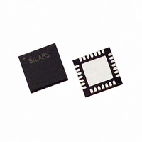
C8051F321-GM Silicon Laboratories Inc, C8051F321-GM Datasheet - Page 102

C8051F321-GM
Manufacturer Part Number
C8051F321-GM
Description
IC 8051 MCU 16K FLASH 28MLP
Manufacturer
Silicon Laboratories Inc
Series
C8051F32xr
Datasheets
1.C8051F320-TB.pdf
(250 pages)
2.C8051F321-GMR.pdf
(2 pages)
3.C8051F321-GM.pdf
(256 pages)
Specifications of C8051F321-GM
Program Memory Type
FLASH
Program Memory Size
16KB (16K x 8)
Package / Case
28-VQFN Exposed Pad, 28-HVQFN, 28-SQFN, 28-DHVQFN
Core Processor
8051
Core Size
8-Bit
Speed
25MHz
Connectivity
SMBus (2-Wire/I²C), SPI, UART/USART, USB
Peripherals
Brown-out Detect/Reset, POR, PWM, Temp Sensor, WDT
Number Of I /o
21
Ram Size
2.25K x 8
Voltage - Supply (vcc/vdd)
2.7 V ~ 3.6 V
Data Converters
A/D 13x10b
Oscillator Type
Internal
Operating Temperature
-40°C ~ 85°C
Processor Series
C8051F3x
Core
8051
Data Bus Width
8 bit
Data Ram Size
2.25 KB
Interface Type
I2C/SMBus/SPI/UART/USB
Maximum Clock Frequency
25 MHz
Number Of Programmable I/os
21
Number Of Timers
4
Operating Supply Voltage
2.7 V to 3.6 V
Maximum Operating Temperature
+ 85 C
Mounting Style
SMD/SMT
3rd Party Development Tools
PK51, CA51, A51, ULINK2
Development Tools By Supplier
C8051F320DK
Minimum Operating Temperature
- 40 C
On-chip Adc
13-ch x 10-bit or 17-ch x 10-bit
No. Of I/o's
21
Ram Memory Size
1280Byte
Cpu Speed
25MHz
No. Of Timers
4
Rohs Compliant
Yes
Lead Free Status / RoHS Status
Lead free / RoHS Compliant
For Use With
336-1480 - DAUGHTER CARD TOOLSTCK C8051F321770-1006 - ISP 4PORT FOR SILABS C8051F MCU336-1449 - ADAPTER PROGRAM TOOLSTICK F321336-1260 - DEV KIT FOR C8051F320/F321
Eeprom Size
-
Lead Free Status / Rohs Status
Lead free / RoHS Compliant
Other names
336-1261
Available stocks
Company
Part Number
Manufacturer
Quantity
Price
Company:
Part Number:
C8051F321-GM
Manufacturer:
SiliconL
Quantity:
4 364
Part Number:
C8051F321-GM
Manufacturer:
SILICON LABS/芯科
Quantity:
20 000
Part Number:
C8051F321-GMR
Manufacturer:
SILICON LABS/芯科
Quantity:
20 000
C8051F320/1
10.3. External Reset
The external /RST pin provides a means for external circuitry to force the device into a reset state. Asserting an
active-low signal on the /RST pin generates a reset; an external pull-up and/or decoupling of the /RST pin may be
necessary to avoid erroneous noise-induced resets. See Table 10.1 for complete /RST pin specifications. The PINRSF
flag (RSTSRC.0) is set on exit from an external reset.
10.4. Missing Clock Detector Reset
The Missing Clock Detector (MCD) is a one-shot circuit that is triggered by the system clock. If more than 100 µs
pass between rising edges on the system clock, the one-shot will time out and generate a reset. After a MCD reset, the
MCDRSF flag (RSTSRC.2) will read ‘1’, signifying the MCD as the reset source; otherwise, this bit reads ‘0’. Writ-
ing a ‘1’ to the MCDRSF bit enables the Missing Clock Detector; writing a ‘0’ disables it. The state of the /RST pin
is unaffected by this reset.
10.5. Comparator0 Reset
Comparator0 can be configured as a reset source by writing a ‘1’ to the C0RSEF flag (RSTSRC.5). Comparator0
should be enabled and allowed to settle prior to writing to C0RSEF to prevent any turn-on chatter on the output from
generating an unwanted reset. The Comparator0 reset is active-low: if the non-inverting input voltage (on CP0+) is
less than the inverting input voltage (on CP0-), a system reset is generated. After a Comparator0 reset, the C0RSEF
flag (RSTSRC.5) will read ‘1’ signifying Comparator0 as the reset source; otherwise, this bit reads ‘0’. The state of
the /RST pin is unaffected by this reset.
10.6. PCA Watchdog Timer Reset
The programmable Watchdog Timer (WDT) function of the Programmable Counter Array (PCA) can be used to pre-
vent software from running out of control during a system malfunction. The PCA WDT function can be enabled or
disabled by software as described in
clocked by SYSCLK / 12 following any reset. If a system malfunction prevents user software from updating the
WDT, a reset is generated and the WDTRSF bit (RSTSRC.5) is set to ‘1’. The state of the /RST pin is unaffected by
this reset.
10.7. FLASH Error Reset
If a FLASH read/write/erase or program read targets an illegal address, a system reset is generated. This may occur
due to any of the following:
•
•
•
•
The FERROR bit (RSTSRC.6) is set following a FLASH error reset. The state of the /RST pin is unaffected by this
reset.
102
A FLASH write or erase is attempted above user code space. This occurs when PSWE is set to ‘1’ and a MOVX
write operation is attempted above address 0x3DFF.
A FLASH read is attempted above user code space. This occurs when a MOVC operation is attempted above
address 0x3DFF.
A Program read is attempted above user code space. This occurs when user code attempts to branch to an address
above 0x3DFF.
A FLASH read, write or erase attempt is restricted due to a FLASH security setting (see
Options” on page
109).
Section “20.3. Watchdog Timer Mode” on page
Rev. 1.1
246; the WDT is enabled and
Section “11.3. Security


