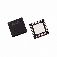
C8051F321-GM Silicon Laboratories Inc, C8051F321-GM Datasheet - Page 218

C8051F321-GM
Manufacturer Part Number
C8051F321-GM
Description
IC 8051 MCU 16K FLASH 28MLP
Manufacturer
Silicon Laboratories Inc
Series
C8051F32xr
Datasheets
1.C8051F320-TB.pdf
(250 pages)
2.C8051F321-GMR.pdf
(2 pages)
3.C8051F321-GM.pdf
(256 pages)
Specifications of C8051F321-GM
Program Memory Type
FLASH
Program Memory Size
16KB (16K x 8)
Package / Case
28-VQFN Exposed Pad, 28-HVQFN, 28-SQFN, 28-DHVQFN
Core Processor
8051
Core Size
8-Bit
Speed
25MHz
Connectivity
SMBus (2-Wire/I²C), SPI, UART/USART, USB
Peripherals
Brown-out Detect/Reset, POR, PWM, Temp Sensor, WDT
Number Of I /o
21
Ram Size
2.25K x 8
Voltage - Supply (vcc/vdd)
2.7 V ~ 3.6 V
Data Converters
A/D 13x10b
Oscillator Type
Internal
Operating Temperature
-40°C ~ 85°C
Processor Series
C8051F3x
Core
8051
Data Bus Width
8 bit
Data Ram Size
2.25 KB
Interface Type
I2C/SMBus/SPI/UART/USB
Maximum Clock Frequency
25 MHz
Number Of Programmable I/os
21
Number Of Timers
4
Operating Supply Voltage
2.7 V to 3.6 V
Maximum Operating Temperature
+ 85 C
Mounting Style
SMD/SMT
3rd Party Development Tools
PK51, CA51, A51, ULINK2
Development Tools By Supplier
C8051F320DK
Minimum Operating Temperature
- 40 C
On-chip Adc
13-ch x 10-bit or 17-ch x 10-bit
No. Of I/o's
21
Ram Memory Size
1280Byte
Cpu Speed
25MHz
No. Of Timers
4
Rohs Compliant
Yes
Lead Free Status / RoHS Status
Lead free / RoHS Compliant
For Use With
336-1480 - DAUGHTER CARD TOOLSTCK C8051F321770-1006 - ISP 4PORT FOR SILABS C8051F MCU336-1449 - ADAPTER PROGRAM TOOLSTICK F321336-1260 - DEV KIT FOR C8051F320/F321
Eeprom Size
-
Lead Free Status / Rohs Status
Lead free / RoHS Compliant
Other names
336-1261
Available stocks
Company
Part Number
Manufacturer
Quantity
Price
Company:
Part Number:
C8051F321-GM
Manufacturer:
SiliconL
Quantity:
4 364
Part Number:
C8051F321-GM
Manufacturer:
SILICON LABS/芯科
Quantity:
20 000
Part Number:
C8051F321-GMR
Manufacturer:
SILICON LABS/芯科
Quantity:
20 000
C8051F320/1
Setting the TR0 bit (TCON.4) enables the timer when either GATE0 (TMOD.3) is logic 0 or the input signal /INT0 is
active as defined by bit IN0PL in register INT01CF (see Figure 8.13). Setting GATE0 to ‘1’ allows the timer to be
controlled by the external input signal /INT0 (see
facilitating pulse width measurements.
Setting TR0 does not force the timer to reset. The timer registers should be loaded with the desired initial value before
the timer is enabled.
TL1 and TH1 form the 13-bit register for Timer 1 in the same manner as described above for TL0 and TH0. Timer 1
is configured and controlled using the relevant TCON and TMOD bits just as with Timer 0. The input signal /INT1 is
used with Timer 1; the /INT1 polarity is defined by bit IN1PL in register INT01CF (see Figure 8.13).
19.1.2. Mode 1: 16-bit Counter/Timer
Mode 1 operation is the same as Mode 0, except that the counter/timer registers use all 16 bits. The counter/timers are
enabled and configured in Mode 1 in the same manner as for Mode 0.
218
/INT0
TR0
T0
X = Don't Care
0
1
1
1
Crossbar
GATE0
Pre-scaled Clock
X
0
1
1
SYSCLK
IN0PL
GATE0
/INT0
XOR
X
X
0
1
Figure 19.1. T0 Mode 0 Block Diagram
TR0
0
1
Counter/Timer
M
H
T
3
M
T
3
L
CKCON
M
H
T
2
Disabled
Disabled
Enabled
Enabled
M
T
2
L
0
1
M
T
1
M
T
0
Section “8.3.5. Interrupt Register Descriptions” on page
S
C
A
1
S
C
A
Rev. 1.1
0
G
A
T
E
1
C
T
1
/
M
T
1
1
TMOD
M
T
1
0
TCLK
G
A
T
E
0
C
T
0
/
M
T
0
1
M
T
0
0
(5 bits)
TL0
N
1
P
L
I
N
S
1
L
2
I
INT01CF
N
S
1
L
1
I
N
S
1
L
0
I
N
P
0
L
I
(8 bits)
TH0
N
0
S
L
2
I
N
0
S
L
1
I
N
0
S
L
0
I
TR1
TR0
TF1
TF0
IE1
IE0
IT1
IT0
Interrupt
61),


