HD64F3687GFPV Renesas Electronics America, HD64F3687GFPV Datasheet - Page 227
HD64F3687GFPV
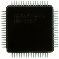
Manufacturer Part Number
HD64F3687GFPV
Description
IC H8 MCU FLASH 56K 64LQFP
Manufacturer
Renesas Electronics America
Series
H8® H8/300H Tinyr
Specifications of HD64F3687GFPV
Core Processor
H8/300H
Core Size
16-Bit
Speed
20MHz
Connectivity
I²C, SCI
Peripherals
LVD, POR, PWM, WDT
Number Of I /o
45
Program Memory Size
56KB (56K x 8)
Program Memory Type
FLASH
Ram Size
4K x 8
Voltage - Supply (vcc/vdd)
3 V ~ 5.5 V
Data Converters
A/D 8x10b
Oscillator Type
Internal
Operating Temperature
-20°C ~ 75°C
Package / Case
64-LQFP
Package
64LQFP
Family Name
H8
Maximum Speed
20 MHz
Operating Supply Voltage
3.3|5 V
Data Bus Width
16|32 Bit
Number Of Programmable I/os
45
Interface Type
I2C/SCI
On-chip Adc
8-chx10-bit
Number Of Timers
3
For Use With
R0K436079S000BE - KIT DEV FOR H8/36079 W/COMPILER
Lead Free Status / RoHS Status
Lead free / RoHS Compliant
Eeprom Size
-
Available stocks
Company
Part Number
Manufacturer
Quantity
Price
Company:

Part Number:
HD64F3687GFPV
Manufacturer:
Renesas Electronics America
Quantity:
10 000


TIORC: TIORC selects whether GRC or GRD is used as an output compare register or an input
capture register. When an output compare register is selected, the output setting is selected. When
an input capture register is selected, an input edge of an input capture signal is selected. TIORC
also selects the function of FTIOC or FTIOD pin.
Legend: X: Don't care
Bit
7
6
5
4
3
2
1
0
Bit Name
IOD2
IOD1
IOD0
IOC2
IOC1
IOC0
Initial
value
1
0
0
0
1
0
0
0
R/W
R/W
R/W
R/W
R/W
R/W
R/W
Description
Reserved
This bit is always read as 1.
I/O Control D2 to D0
GRD is an output compare register:
000: Disables pin output by compare match
001: 0 output by GRD compare match
010: 1 output by GRD compare match
011: Toggle output by GRD compare match
GRD is an input capture register:
100: Input capture to GRD at the rising edge
101: Input capture to GRD at the falling edge
11X: Input capture to GRD at both rising and falling
Reserved
This bit is always read as 1.
I/O Control C2 to C0
GRC is an output compare register:
000: Disables pin output by compare match
001: 0 output by GRC compare match
010: 1 output by GRC compare match
011: Toggle Output by GRC compare match
GRC is an input capture register:
100: Input capture to GRC at the rising edge
101: Input capture to GRC at the falling edge
11X: Input capture to GRC at both rising and falling
edges
edges
Rev.5.00 Nov. 02, 2005 Page 193 of 500
Section 13 Timer Z
REJ09B0027-0500
Related parts for HD64F3687GFPV
Image
Part Number
Description
Manufacturer
Datasheet
Request
R


Part Number:
Description:
KIT STARTER FOR M16C/29
Manufacturer:
Renesas Electronics America
Datasheet:

Part Number:
Description:
KIT STARTER FOR R8C/2D
Manufacturer:
Renesas Electronics America
Datasheet:

Part Number:
Description:
R0K33062P STARTER KIT
Manufacturer:
Renesas Electronics America
Datasheet:

Part Number:
Description:
KIT STARTER FOR R8C/23 E8A
Manufacturer:
Renesas Electronics America
Datasheet:

Part Number:
Description:
KIT STARTER FOR R8C/25
Manufacturer:
Renesas Electronics America
Datasheet:

Part Number:
Description:
KIT STARTER H8S2456 SHARPE DSPLY
Manufacturer:
Renesas Electronics America
Datasheet:

Part Number:
Description:
KIT STARTER FOR R8C38C
Manufacturer:
Renesas Electronics America
Datasheet:

Part Number:
Description:
KIT STARTER FOR R8C35C
Manufacturer:
Renesas Electronics America
Datasheet:

Part Number:
Description:
KIT STARTER FOR R8CL3AC+LCD APPS
Manufacturer:
Renesas Electronics America
Datasheet:
Part Number:
Description:
KIT STARTER FOR RX610
Manufacturer:
Renesas Electronics America
Datasheet:

Part Number:
Description:
KIT STARTER FOR R32C/118
Manufacturer:
Renesas Electronics America
Datasheet:

Part Number:
Description:
KIT DEV RSK-R8C/26-29
Manufacturer:
Renesas Electronics America
Datasheet:

Part Number:
Description:
KIT STARTER FOR SH7124
Manufacturer:
Renesas Electronics America
Datasheet:

Part Number:
Description:
KIT STARTER FOR H8SX/1622
Manufacturer:
Renesas Electronics America
Datasheet: