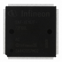
SAF-XE167F-72F66L AC Infineon Technologies, SAF-XE167F-72F66L AC Datasheet - Page 98

SAF-XE167F-72F66L AC
Manufacturer Part Number
SAF-XE167F-72F66L AC
Description
IC MCU 16BIT FLASH PG-LQFP-144
Manufacturer
Infineon Technologies
Series
XE16xr
Datasheet
1.SAF-XE167K-96F66L_AC.pdf
(122 pages)
Specifications of SAF-XE167F-72F66L AC
Core Processor
C166SV2
Core Size
16-Bit
Speed
66MHz
Connectivity
CAN, EBI/EMI, I²C, LIN, SPI, SSC, UART/USART, USI
Peripherals
I²S, POR, PWM, WDT
Number Of I /o
118
Program Memory Size
576KB (576K x 8)
Program Memory Type
FLASH
Ram Size
50K x 8
Voltage - Supply (vcc/vdd)
3 V ~ 5.5 V
Data Converters
A/D 24x10b
Oscillator Type
Internal
Operating Temperature
-40°C ~ 85°C
Package / Case
144-LFQFP
Data Bus Width
16 bit
Data Ram Size
32 KB
Interface Type
CAN
Maximum Clock Frequency
66 MHz
Number Of Programmable I/os
118
Number Of Timers
11
Maximum Operating Temperature
+ 85 C
Mounting Style
SMD/SMT
Minimum Operating Temperature
- 40 C
On-chip Adc
10 bit, 24 Channel
Lead Free Status / RoHS Status
Lead free / RoHS Compliant
Eeprom Size
-
Lead Free Status / Rohs Status
Details
Other names
FXE167F72F66LACXP
SAF-XE167F-72F66LACIN
SP000363813
SAF-XE167F-72F66LACIN
SP000363813
The timing in the AC Characteristics refers to TCSs. Timing must be calculated using the
minimum TCS possible under the given circumstances.
The actual minimum value for TCS depends on the jitter of the PLL. Because the PLL is
constantly adjusting its output frequency to correspond to the input frequency (from
crystal or oscillator), the accumulated jitter is limited. This means that the relative
deviation for periods of more than one TCS is lower than for a single TCS (see formulas
and
This is especially important for bus cycles using waitstates and for the operation of
timers, serial interfaces, etc. For all slower operations and longer periods (e.g. pulse train
generation or measurement, lower baudrates, etc.) the deviation caused by the PLL jitter
is negligible.
The value of the accumulated PLL jitter depends on the number of consecutive VCO
output cycles within the respective timeframe. The VCO output clock is divided by the
output prescaler K2 to generate the system clock signal
is K2 × T, where T is the number of consecutive
The maximum accumulated jitter (long-term jitter) D
D
This maximum value is applicable, if either the number of clock cycles T > (
the prescaler value K2 > 17.
In all other cases for a timeframe of T × TCS the accumulated jitter D
D
f
Example, for a period of 3 TCSs @ 33 MHz and K2 = 4:
D
D
= 5.97 × [0.768 × 2 / 26.39 + 0.232]
= 1.7 ns
Example, for a period of 3 TCSs @ 33 MHz and K2 = 2:
D
D
= 7.63 × [0.884 × 2 / 26.39 + 0.116]
= 1.4 ns
Data Sheet
SYS
Tmax
T
max
3
max
3
= 5.97 × [(1 - 0.058 × 4) × (3 - 1) / (0.83 × 33 - 1) + 0.058 × 4]
= 7.63 × [(1 - 0.058 × 2) × (3 - 1) / (0.83 × 33 - 1) + 0.058 × 2]
[ns] = D
Figure
in [MHz] in all formulas.
= ±(220 / (4 × 33) + 4.3) = 5.97 ns (Not applicable directly in this case!)
= ±(220 / (2 × 33) + 4.3) = 7.63 ns (Not applicable directly in this case!)
[ns] = ±(220 / (K2 ×
Tmax
19).
× [(1 - 0.058 × K2) × (T - 1) / (0.83 ×
f
SYS
) + 4.3)
96
f
SYS
Tmax
f
cycles (TCS).
SYS
f
SYS
is defined by:
XE166 Family Derivatives
- 1) + 0.058 × K2]
. The number of VCO cycles
Electrical Parameters
T
is determined by:
V2.1, 2008-08
f
SYS
XE167x
/ 1.2) or


