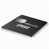
EP9302-IQZ Cirrus Logic Inc, EP9302-IQZ Datasheet - Page 499

EP9302-IQZ
Manufacturer Part Number
EP9302-IQZ
Description
IC ARM9 SOC PROCESSOR 208LQFP
Manufacturer
Cirrus Logic Inc
Series
EP9r
Datasheets
1.EP9307-CRZ.pdf
(824 pages)
2.EP9302-IQZ.pdf
(42 pages)
3.EP9302-IQZ.pdf
(4 pages)
4.EP9302-IQZ.pdf
(40 pages)
Specifications of EP9302-IQZ
Core Size
16/32-Bit
Core Processor
ARM9
Speed
200MHz
Connectivity
EBI/EMI, Ethernet, I²C, IrDA, SPI, UART/USART, USB
Peripherals
AC'97, DMA, I²:S, LED, MaverickKey, POR, PWM, WDT
Number Of I /o
19
Program Memory Type
ROMless
Ram Size
32K x 8
Voltage - Supply (vcc/vdd)
1.65 V ~ 3.6 V
Data Converters
A/D 5x12b
Oscillator Type
External
Operating Temperature
-40°C ~ 85°C
Package / Case
208-LQFP
Controller Family/series
(ARM9)
No. Of I/o's
19
Ram Memory Size
16MB
Cpu Speed
200MHz
No. Of Timers
3
No. Of Pwm Channels
1
Digital Ic Case Style
LQFP
Embedded Interface Type
AC97, I2S, SPI, UART, USB
Rohs Compliant
Yes
Processor Series
EP93xx
Core
ARM920T
Data Bus Width
32 bit
Mounting Style
SMD/SMT
3rd Party Development Tools
MDK-ARM, RL-ARM, ULINK2
Development Tools By Supplier
EDB9302A-Z
Lead Free Status / RoHS Status
Lead free / RoHS Compliant
For Use With
598-1132 - KIT DEVELOPMENT EP9302 ARM9
Eeprom Size
-
Program Memory Size
-
Lead Free Status / Rohs Status
Details
Other names
598-1253
Available stocks
Company
Part Number
Manufacturer
Quantity
Price
Part Number:
EP9302-IQZ
Manufacturer:
CIRRUS
Quantity:
20 000
- EP9307-CRZ PDF datasheet
- EP9302-IQZ PDF datasheet #2
- EP9302-IQZ PDF datasheet #3
- EP9302-IQZ PDF datasheet #4
- Current page: 499 of 824
- Download datasheet (13Mb)
DS785UM1
13.3 Address Pin Usage
Each of the four synchronous memory domains can be fitted with a variety of device types,
provided the total capacitance on any address/control/data line does not exceed the specified
operating limit. Four pins, SDCSn[3:0], are used to as chip-selects (domain selects) for the
four synchronous memory domains, where the configurations of the domains are specified by
registers SDRAMDevCfg[3:0], SDRAMDevCfg[3:0], SDRAMDevCfg[3:0], and
SDRAMDevCfg[3:0], respectively. For example, SDCSn[2] selects the 3rd of four
synchronous memory domains and SDRAMDevCfg[3:0] specifies the configuration of that
domain.
Address bits 31:28 are internally decoded to specify an address domain.
he values of address bits 31:28 that specify a synchronous memory domain.
Because of the row/column/bank architecture of synchronous memory devices, the mapping
of these memories into the processor’s memory space is not always obvious, typically
because the memory inside a synchronous device does not appear to the processor to be
continuous. For example, a 32-Mbyte SDRAM device may be visible as four 4-Mbyte banks.
Table 13-3
internal address signals are identified as A[27:1]. The 2nd row of the table shows the address
pins, AD[15:0], that may be connected to the synchronous memory device, depending on its
address depth. The remaining rows show how the device’s linear address space is mapped
onto the address pins, AD[15:0]. For each memory device configuration, that is, 16- or 32-bit
wide SDRAM or SROM or SFLASH, there is a Row and Bank, and Column, entry in the table
that shows the internal linear address bits, A[27:1], that are presented on the external
AD[15:0] pins for Row and Bank, and Column, accesses. The shallower the depth of the
synchronous memory device, the fewer the number of most-significant address bits that are
used for Row and Bank, and Column, addressing. By observing the number of rows and
columns in a specific synchronous memory device (see the device’s data sheet), the actual
number of address bits used for addressing the device can be determined. Because some
address bits are not used, the address map of the synchronous memory appears to be non-
continuous. The SROMLL should be used when possible to reduce the number of “holes” in
it’s data outputs in the high impedance state. If power-on reset has become de-
asserted, the ARM Core is released from the reset state.
Value of Address
shows address pin usage. In
0xB through 0x1
Bits 31:28
Table 13-2. Address Decoding for Synchronous Memory Domains
0xF
0xE
0xD
0xC
0x0
SDCSn[3:0]
Copyright 2007 Cirrus Logic
None
3
2
1
0
3
Table
Used for other domains
Used during boot from SyncROM or
SyncFLASH
Synchronous Memory Domain
13-3, external pins are identified as AD[15:0],
SDRAM, SyncROM, and SyncFLASH Controller
4
3
2
1
Table 13-2
EP93xx User’s Guide
shows
13-3
13
Related parts for EP9302-IQZ
Image
Part Number
Description
Manufacturer
Datasheet
Request
R

Part Number:
Description:
IC ARM9 SOC PROCESSOR 208LQFP
Manufacturer:
Cirrus Logic Inc
Datasheet:

Part Number:
Description:
High Performance, Entry Level ARM9 SoC
Manufacturer:
Cirrus Logic Inc

Part Number:
Description:
MCU, MPU & DSP Development Tools Eval Bd Hgh-Prfrmnc ARM9 SOC Processor
Manufacturer:
Cirrus Logic Inc
Datasheet:

Part Number:
Description:
Development Kit
Manufacturer:
Cirrus Logic Inc
Datasheet:

Part Number:
Description:
Development Kit
Manufacturer:
Cirrus Logic Inc
Datasheet:

Part Number:
Description:
High-efficiency PFC + Fluorescent Lamp Driver Reference Design
Manufacturer:
Cirrus Logic Inc
Datasheet:

Part Number:
Description:
Development Kit
Manufacturer:
Cirrus Logic Inc
Datasheet:

Part Number:
Description:
Development Kit
Manufacturer:
Cirrus Logic Inc
Datasheet:

Part Number:
Description:
Development Kit
Manufacturer:
Cirrus Logic Inc
Datasheet:

Part Number:
Description:
Development Kit
Manufacturer:
Cirrus Logic Inc
Datasheet:

Part Number:
Description:
Development Kit
Manufacturer:
Cirrus Logic Inc
Datasheet:

Part Number:
Description:
Ref Bd For Speakerbar MSA & DSP Products
Manufacturer:
Cirrus Logic Inc


