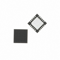
C8051T635-GM Silicon Laboratories Inc, C8051T635-GM Datasheet - Page 49

C8051T635-GM
Manufacturer Part Number
C8051T635-GM
Description
IC MCU 2KB 20PIN QFN
Manufacturer
Silicon Laboratories Inc
Series
C8051T63xr
Specifications of C8051T635-GM
Program Memory Type
OTP
Program Memory Size
2KB (2K x 8)
Package / Case
20-QFN
Core Processor
8051
Core Size
8-Bit
Speed
25MHz
Connectivity
SMBus (2-Wire/I²C), SPI, UART/USART
Peripherals
POR, PWM, WDT
Number Of I /o
17
Ram Size
768 x 8
Voltage - Supply (vcc/vdd)
1.8 V ~ 3.6 V
Oscillator Type
Internal
Operating Temperature
-40°C ~ 85°C
Processor Series
C8051T6x
Core
8051
Data Bus Width
8 bit
Data Ram Size
768 B
Interface Type
I2C/SPI/UART
Maximum Clock Frequency
25 MHz
Number Of Programmable I/os
17
Number Of Timers
4
Operating Supply Voltage
1.8 V to 3.6 V
Maximum Operating Temperature
+ 85 C
Mounting Style
SMD/SMT
3rd Party Development Tools
PK51, CA51, A51, ULINK2
Development Tools By Supplier
C8051T630DK
Minimum Operating Temperature
- 40 C
Package
20QFN EP
Device Core
8051
Family Name
C8051T63x
Maximum Speed
25 MHz
Lead Free Status / RoHS Status
Lead free / RoHS Compliant
For Use With
336-1464 - KIT DEV FOR C8051T630 FAMILY
Eeprom Size
-
Data Converters
-
Lead Free Status / Rohs Status
Lead free / RoHS Compliant
Other names
336-1463-5
Available stocks
Company
Part Number
Manufacturer
Quantity
Price
Company:
Part Number:
C8051T635-GM
Manufacturer:
Silicon
Quantity:
750
8.1.2. Update Output Based on Timer Overflow
Similar to the ADC operation, in which an ADC conversion can be initiated by a timer overflow indepen-
dently of the processor, the IDAC outputs can use a Timer overflow to schedule an output update event.
This feature is useful in systems where the IDAC is used to generate a waveform of a defined sampling
rate by eliminating the effects of variable interrupt latency and instruction execution on the timing of the
IDAC output. When the IDA0CM bits (IDA0CN.[6:4]) are set to 000, 001, 010 or 011, writes to both IDAC
data registers (IDA0L and IDA0H) are held until an associated Timer overflow event (Timer 0, Timer 1,
Timer 2 or Timer 3, respectively) occurs, at which time the IDA0H:IDA0L contents are copied to the IDAC
input latches, allowing the IDAC output to change to the new value.
8.1.3. Update Output Based on CNVSTR Edge
The IDAC output can also be configured to update on a rising edge, falling edge, or both edges of the
external CNVSTR signal. When the IDA0CM bits (IDA0CN.[6:4]) are set to 100, 101, or 110, writes to both
IDAC data registers (IDA0L and IDA0H) are held until an edge occurs on the CNVSTR input pin. The par-
ticular setting of the IDA0CM bits determines whether IDAC outputs are updated on rising, falling, or both
edges of CNVSTR. When a corresponding edge occurs, the IDA0H:IDA0L contents are copied to the IDAC
input latches, allowing the IDAC output to change to the new value.
8.2. IDAC Output Mapping
The IDAC data registers (IDA0H and IDA0L) are left-justified, meaning that the eight MSBs of the IDAC
output word are mapped to bits 7–0 of the IDA0H register, and the two LSBs of the IDAC output word are
mapped to bits 7 and 6 of the IDA0L register. The data word mapping for the IDAC is shown in Figure 8.2.
The full-scale output current of the IDAC is selected using the IDA0OMD bits (IDA0CN[1:0]). By default,
the IDAC is set to a full-scale output current of 2 mA. The IDA0OMD bits can also be configured to provide
full-scale output currents of 1 mA or 0.5 mA, as shown in SFR Definition 8.1.
Input Data Word
B9
(IDA09–IDA00)
0x3FF
0x000
0x001
0x200
B8
B7
B6
IDA0H
IDA0OMD[1:0] = 1x
1023/1024 x 2 mA
512/1024 x 2 mA
Output Current
1/1024 x 2 mA
B5
Figure 8.2. IDA0 Data Word Mapping
0 mA
B4
B3
B2
Rev. 1.0
IDA0OMD[1:0] = 01
1023/1024 x 1 mA
512/1024 x 1 mA
B1
Output Current
1/1024 x 1 mA
0 mA
B0
C8051T630/1/2/3/4/5
IDA0L
IDA0OMD[1:0] = 00
1023/1024 x 0.5 mA
512/1024 x 0.5 mA
1/1024 x 0.5 mA
Output Current
0 mA
49


