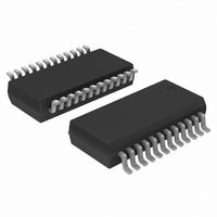
C8051F901-GU Silicon Laboratories Inc, C8051F901-GU Datasheet - Page 209

C8051F901-GU
Manufacturer Part Number
C8051F901-GU
Description
IC MCU 8BIT 8KB FLASH 24QSOP
Manufacturer
Silicon Laboratories Inc
Series
C8051F9xxr
Specifications of C8051F901-GU
Program Memory Type
FLASH
Program Memory Size
8KB (8K x 8)
Package / Case
24-QSOP
Core Processor
8051
Core Size
8-Bit
Speed
25MHz
Connectivity
SMBus (2-Wire/I²C), SPI, UART/USART
Peripherals
Brown-out Detect/Reset, POR, PWM, Temp Sensor, WDT
Number Of I /o
16
Ram Size
768 x 8
Voltage - Supply (vcc/vdd)
0.9 V ~ 3.6 V
Data Converters
A/D 15x10b
Oscillator Type
Internal
Operating Temperature
-40°C ~ 85°C
Processor Series
C8051F9x
Core
8051
Data Ram Size
768 B
Interface Type
UART
Maximum Clock Frequency
25 MHz
Number Of Timers
4
Operating Supply Voltage
0.9 V to 3.6 V
Maximum Operating Temperature
+ 85 C
Mounting Style
SMD/SMT
3rd Party Development Tools
PK51, CA51, A51, ULINK2
Development Tools By Supplier
C8051F912DK
Minimum Operating Temperature
- 40 C
On-chip Adc
10 bit
Package
24QSOP
Device Core
8051
Family Name
C8051F90x
Maximum Speed
25 MHz
Data Bus Width
8 Bit
Number Of Programmable I/os
16
Lead Free Status / RoHS Status
Lead free / RoHS Compliant
Eeprom Size
-
Lead Free Status / Rohs Status
Lead free / RoHS Compliant
Other names
336-1847-5
Available stocks
Company
Part Number
Manufacturer
Quantity
Price
Company:
Part Number:
C8051F901-GU
Manufacturer:
Silicon Laboratories Inc
Quantity:
135
- Current page: 209 of 318
- Download datasheet (3Mb)
21.3. Priority Crossbar Decoder
The Priority Crossbar Decoder assigns a Port I/O pin to each software selected digital function using the
fixed peripheral priority order shown in Figure 21.3. The registers XBR0, XBR1, and XBR2 defined in SFR
Definition 21.1, SFR Definition 21.2, and SFR Definition 21.3 are used to select digital functions in the
Crossbar. The Port pins available for assignment by the Crossbar include all Port pins (P0.0–P1.6) which
have their corresponding bit in PnSKIP set to 0.
From Figure 21.3, the highest priority peripheral is UART0. If UART0 is selected in the Crossbar (using the
XBRn registers), then P0.4 and P0.5 will be assigned to UART0. The next highest priority peripheral is
SPI1. If SPI1 is selected in the Crossbar, then P1.0–P1.3 will be assigned to SPI1. The user should ensure
that the pins to be assigned by the Crossbar have their PnSKIP bits set to 0.
For all remaining digital functions selected in the Crossbar, starting at the top of Figure 21.3 going down,
the least-significant unskipped, unassigned Port pin(s) are assigned to that function. If a Port pin is already
assigned (e.g. UART0 or SPI1 pins), or if its PnSKIP bit is set to 1, then the Crossbar will skip over the pin
and find next available unskipped, unassigned Port pin. All Port pins used for analog functions, GPIO, or
dedicated digital functions such as the EMIF should have their PnSKIP bit set to 1.
Figure 21.3 shows the Crossbar Decoder priority with no Port pins skipped (P0SKIP, P1SKIP = 0x00);
Figure 21.4 shows the Crossbar Decoder priority with the External Oscillator pins (XTAL1 and XTAL2)
skipped (P0SKIP = 0x0C).
Notes:
•
•
•
•
The Crossbar must be enabled (XBARE = 1) before any Port pin is used as a digital output. Port output drivers are
disabled while the Crossbar is disabled.
When SMBus is selected in the Crossbar, the pins associated with SDA and SCL will automatically be forced into
open-drain output mode regardless of the PnMDOUT setting.
SPI0 can be operated in either 3-wire or 4-wire modes, depending on the state of the NSSMD1-NSSMD0 bits in
register SPI0CN. The NSS signal is only routed to a Port pin when 4-wire mode is selected. When SPI0 is
selected in the Crossbar, the SPI0 mode (3-wire or 4-wire) will affect the pinout of all digital functions lower in pri-
ority than SPI0.
For given XBRn, PnSKIP, and SPInCN register settings, one can determine the I/O pin-out of the device using
Figure 21.3 and Figure 21.4.
Rev. 1.0
C8051F91x-C8051F90x
209
Related parts for C8051F901-GU
Image
Part Number
Description
Manufacturer
Datasheet
Request
R
Part Number:
Description:
SMD/C°/SINGLE-ENDED OUTPUT SILICON OSCILLATOR
Manufacturer:
Silicon Laboratories Inc
Part Number:
Description:
Manufacturer:
Silicon Laboratories Inc
Datasheet:
Part Number:
Description:
N/A N/A/SI4010 AES KEYFOB DEMO WITH LCD RX
Manufacturer:
Silicon Laboratories Inc
Datasheet:
Part Number:
Description:
N/A N/A/SI4010 SIMPLIFIED KEY FOB DEMO WITH LED RX
Manufacturer:
Silicon Laboratories Inc
Datasheet:
Part Number:
Description:
N/A/-40 TO 85 OC/EZLINK MODULE; F930/4432 HIGH BAND (REV E/B1)
Manufacturer:
Silicon Laboratories Inc
Part Number:
Description:
EZLink Module; F930/4432 Low Band (rev e/B1)
Manufacturer:
Silicon Laboratories Inc
Part Number:
Description:
I°/4460 10 DBM RADIO TEST CARD 434 MHZ
Manufacturer:
Silicon Laboratories Inc
Part Number:
Description:
I°/4461 14 DBM RADIO TEST CARD 868 MHZ
Manufacturer:
Silicon Laboratories Inc
Part Number:
Description:
I°/4463 20 DBM RFSWITCH RADIO TEST CARD 460 MHZ
Manufacturer:
Silicon Laboratories Inc
Part Number:
Description:
I°/4463 20 DBM RADIO TEST CARD 868 MHZ
Manufacturer:
Silicon Laboratories Inc
Part Number:
Description:
I°/4463 27 DBM RADIO TEST CARD 868 MHZ
Manufacturer:
Silicon Laboratories Inc
Part Number:
Description:
I°/4463 SKYWORKS 30 DBM RADIO TEST CARD 915 MHZ
Manufacturer:
Silicon Laboratories Inc
Part Number:
Description:
N/A N/A/-40 TO 85 OC/4463 RFMD 30 DBM RADIO TEST CARD 915 MHZ
Manufacturer:
Silicon Laboratories Inc
Part Number:
Description:
I°/4463 20 DBM RADIO TEST CARD 169 MHZ
Manufacturer:
Silicon Laboratories Inc


