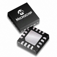
PIC16F688-E/ML Microchip Technology, PIC16F688-E/ML Datasheet - Page 223

PIC16F688-E/ML
Manufacturer Part Number
PIC16F688-E/ML
Description
IC PIC MCU FLASH 4KX14 16QFN
Manufacturer
Microchip Technology
Series
PIC® 16Fr
Datasheets
1.PIC16F616T-ISL.pdf
(8 pages)
2.PIC16F688T-ISL.pdf
(204 pages)
3.PIC16F688T-ISL.pdf
(6 pages)
4.PIC16F688T-ISL.pdf
(4 pages)
5.PIC16F688T-ISL.pdf
(688 pages)
Specifications of PIC16F688-E/ML
Core Size
8-Bit
Program Memory Size
7KB (4K x 14)
Core Processor
PIC
Speed
20MHz
Connectivity
UART/USART
Peripherals
Brown-out Detect/Reset, POR, WDT
Number Of I /o
12
Program Memory Type
FLASH
Eeprom Size
256 x 8
Ram Size
256 x 8
Voltage - Supply (vcc/vdd)
2 V ~ 5.5 V
Data Converters
A/D 8x10b
Oscillator Type
Internal
Operating Temperature
-40°C ~ 125°C
Package / Case
16-QFN
Controller Family/series
PIC16F
No. Of I/o's
12
Eeprom Memory Size
256Byte
Ram Memory Size
256Byte
Cpu Speed
20MHz
No. Of Timers
2
Processor Series
PIC16F
Core
PIC
Data Bus Width
8 bit
Data Ram Size
256 B
Interface Type
EUSART, RS- 232, SCI, USB
Maximum Clock Frequency
20 MHz
Number Of Programmable I/os
12
Number Of Timers
2
Maximum Operating Temperature
+ 125 C
Mounting Style
SMD/SMT
3rd Party Development Tools
52715-96, 52716-328, 52717-734
Development Tools By Supplier
PG164130, DV164035, DV244005, DV164005, PG164120, ICE2000, DM163014, DM164120-4
Minimum Operating Temperature
- 40 C
On-chip Adc
10 bit, 8 Channel
Lead Free Status / RoHS Status
Lead free / RoHS Compliant
For Use With
AC164324 - MODULE SKT FOR MPLAB 8DFN/16QFNXLT16QFN1 - SOCKET TRANSITION 14DIP TO 16QFNAC162061 - HEADER INTRFC MPLAB ICD2 20PINAC162056 - HEADER INTERFACE ICD2 16F688
Lead Free Status / Rohs Status
Details
- PIC16F616T-ISL PDF datasheet
- PIC16F688T-ISL PDF datasheet #2
- PIC16F688T-ISL PDF datasheet #3
- PIC16F688T-ISL PDF datasheet #4
- PIC16F688T-ISL PDF datasheet #5
- Current page: 223 of 688
- Download datasheet (3Mb)
15.2
1997 Microchip Technology Inc.
Control Registers
bit 7
bit 6
bit 5
bit 4
bit 3
bit 2
bit 1
bit 0
Register 15-1: SSPSTAT: Synchronous Serial Port Status Register
bit 7
SMP: SPI data input sample phase
SPI Master Mode
1 = Input data sampled at end of data output time
0 = Input data sampled at middle of data output time
SPI Slave Mode
SMP must be cleared when SPI is used in slave mode
CKE: SPI Clock Edge Select
CKP = 0 (SSPCON<4>)
1 = Data transmitted on rising edge of SCK
0 = Data transmitted on falling edge of SCK
CKP = 1 (SSPCON<4>)
1 = Data transmitted on falling edge of SCK
0 = Data transmitted on rising edge of SCK
D/A: Data/Address bit (I
1 = Indicates that the last byte received or transmitted was data
0 = Indicates that the last byte received or transmitted was address
P: Stop bit
(I
1 = Indicates that a stop bit has been detected last (this bit is '0' on RESET)
0 = Stop bit was not detected last
S: Start bit
(I
1 = Indicates that a start bit has been detected last (this bit is '0' on RESET)
0 = Start bit was not detected last
R/W: Read/Write bit information (I
This bit holds the R/W bit information following the last address match. This bit is only valid from
the address match to the next start bit, stop bit, or not ACK bit.
1 = Read
0 = Write
UA: Update Address (10-bit I
1 = Indicates that the user needs to update the address in the SSPADD register
0 = Address does not need to be updated
BF: Buffer Full Status bit
Receive (SPI and I
1 = Receive complete, SSPBUF is full
0 = Receive not complete, SSPBUF is empty
Transmit (I
1 = Transmit in progress, SSPBUF is full
0 = Transmit complete, SSPBUF is empty
Legend
R = Readable bit
U = Unimplemented bit, read as ‘0’
2
2
R/W-0
C mode only. This bit is cleared when the SSP module is disabled)
C mode only. This bit is cleared when the SSP module is disabled)
SMP
2
C mode only)
R/W-0
CKE
2
C modes)
2
C mode only)
W = Writable bit
R-0
D/A
2
(Figure
C mode only)
2
C mode only)
15-3,
R-0
P
Figure
15-4, and
- n = Value at POR reset
Section 15. SSP
R-0
S
Figure
R/W
R-0
15-5)
DS31015A-page 15-3
R-0
UA
bit 0
R-0
BF
15
Related parts for PIC16F688-E/ML
Image
Part Number
Description
Manufacturer
Datasheet
Request
R

Part Number:
Description:
Manufacturer:
Microchip Technology Inc.
Datasheet:

Part Number:
Description:
IC PIC MCU FLASH 4KX14 14SOIC
Manufacturer:
Microchip Technology
Datasheet:

Part Number:
Description:
IC MCU FLASH 4KX14 14TSSOP
Manufacturer:
Microchip Technology
Datasheet:

Part Number:
Description:
IC PIC MCU FLASH 4KX14 14DIP
Manufacturer:
Microchip Technology
Datasheet:

Part Number:
Description:
IC PIC MCU FLASH 4KX14 16QFN
Manufacturer:
Microchip Technology
Datasheet:

Part Number:
Description:
IC MCU PIC FLASH 4KX14 14SOIC
Manufacturer:
Microchip Technology
Datasheet:

Part Number:
Description:
IC PIC MCU FLASH 4KX14 14TSSOP
Manufacturer:
Microchip Technology
Datasheet:

Part Number:
Description:
IC MCU PIC FLASH 4KX14 14DIP
Manufacturer:
Microchip Technology
Datasheet:

Part Number:
Description:
IC PIC MCU FLASH 4KX14 14TSSOP
Manufacturer:
Microchip Technology
Datasheet:

Part Number:
Description:
IC, 8BIT MCU, PIC16F, 32MHZ, SOIC-18
Manufacturer:
Microchip Technology
Datasheet:

Part Number:
Description:
IC, 8BIT MCU, PIC16F, 32MHZ, SSOP-20
Manufacturer:
Microchip Technology
Datasheet:

Part Number:
Description:
IC, 8BIT MCU, PIC16F, 32MHZ, DIP-18
Manufacturer:
Microchip Technology
Datasheet:

Part Number:
Description:
IC, 8BIT MCU, PIC16F, 32MHZ, QFN-28
Manufacturer:
Microchip Technology
Datasheet:

Part Number:
Description:
IC, 8BIT MCU, PIC16F, 32MHZ, QFN-28
Manufacturer:
Microchip Technology
Datasheet:

Part Number:
Description:
IC, 8BIT MCU, PIC16F, 32MHZ, QFN-28
Manufacturer:
Microchip Technology
Datasheet:


