ATMEGA48-20MU Atmel, ATMEGA48-20MU Datasheet - Page 254
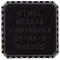
ATMEGA48-20MU
Manufacturer Part Number
ATMEGA48-20MU
Description
IC AVR MCU 4K 20MHZ 5V 32-QFN
Manufacturer
Atmel
Series
AVR® ATmegar
Specifications of ATMEGA48-20MU
Core Processor
AVR
Core Size
8-Bit
Speed
20MHz
Connectivity
I²C, SPI, UART/USART
Peripherals
Brown-out Detect/Reset, POR, PWM, WDT
Number Of I /o
23
Program Memory Size
4KB (2K x 16)
Program Memory Type
FLASH
Eeprom Size
256 x 8
Ram Size
512 x 8
Voltage - Supply (vcc/vdd)
2.7 V ~ 5.5 V
Data Converters
A/D 8x10b
Oscillator Type
Internal
Operating Temperature
-40°C ~ 85°C
Package / Case
32-VQFN Exposed Pad, 32-HVQFN, 32-SQFN, 32-DHVQFN
Processor Series
ATMEGA48x
Core
AVR8
Data Bus Width
8 bit
Data Ram Size
512 B
Interface Type
2-Wire/SPI/USART/Serial
Maximum Clock Frequency
20 MHz
Number Of Programmable I/os
23
Number Of Timers
3
Operating Supply Voltage
2.7 V to 5.5 V
Maximum Operating Temperature
+ 85 C
Mounting Style
SMD/SMT
3rd Party Development Tools
EWAVR, EWAVR-BL
Development Tools By Supplier
ATAVRDRAGON, ATSTK500, ATSTK600, ATAVRISP2, ATAVRONEKIT
Minimum Operating Temperature
- 40 C
On-chip Adc
8-ch x 10-bit
Controller Family/series
AVR MEGA
No. Of I/o's
23
Eeprom Memory Size
256Byte
Ram Memory Size
512Byte
Cpu Speed
20MHz
No. Of Timers
3
Rohs Compliant
Yes
Package
32MLF EP
Device Core
AVR
Family Name
ATmega
Maximum Speed
20 MHz
For Use With
ATSTK600-TQFP32 - STK600 SOCKET/ADAPTER 32-TQFPATSTK600-DIP40 - STK600 SOCKET/ADAPTER 40-PDIP770-1007 - ISP 4PORT ATMEL AVR MCU SPI/JTAGATAVRDRAGON - KIT DRAGON 32KB FLASH MEM AVRATAVRISP2 - PROGRAMMER AVR IN SYSTEMATJTAGICE2 - AVR ON-CHIP D-BUG SYSTEM
Lead Free Status / RoHS Status
Lead free / RoHS Compliant
Available stocks
Company
Part Number
Manufacturer
Quantity
Price
Company:

Part Number:
ATMEGA48-20MU
Manufacturer:
ATMEL
Quantity:
18 000


23.7
23.8
23.8.1
254
ADC Conversion Result
Register Description
ATmega48/88/168
ADMUX – ADC Multiplexer Selection Register
After the conversion is complete (ADIF is high), the conversion result can be found in the ADC
Result Registers (ADCL, ADCH).
For single ended conversion, the result is
where V
Table 23-2 on page 254
0x3FF represents the selected reference voltage minus one LSB.
• Bit 7:6 – REFS1:0: Reference Selection Bits
These bits select the voltage reference for the ADC, as shown in
changed during a conversion, the change will not go in effect until this conversion is complete
(ADIF in ADCSRA is set). The internal voltage reference options may not be used if an external
reference voltage is being applied to the AREF pin.
Table 23-2.
• Bit 5 – ADLAR: ADC Left Adjust Result
The ADLAR bit affects the presentation of the ADC conversion result in the ADC Data Register.
Write one to ADLAR to left adjust the result. Otherwise, the result is right adjusted. Changing the
ADLAR bit will affect the ADC Data Register immediately, regardless of any ongoing conver-
sions. For a complete description of this bit, see
page
• Bit 4 – Res: Reserved Bit
This bit is an unused bit in the ATmega48/88/168, and will always read as zero.
• Bits 3:0 – MUX3:0: Analog Channel Selection Bits
Bit
(0x7C)
Read/Write
Initial Value
REFS1
0
0
1
1
257.
IN
is the voltage on the selected input pin and V
REFS0
REFS1
Voltage Reference Selections for ADC
R/W
0
1
0
1
7
0
REFS0
Voltage Reference Selection
AREF, Internal V
AV
Reserved
Internal 1.1V Voltage Reference with external capacitor at AREF pin
R/W
6
0
and
CC
with external capacitor at AREF pin
Table 23-3 on page
ADLAR
R/W
5
0
ADC
ref
turned off
R
0
4
–
=
V
--------------------------
MUX3
IN
R/W
“ADCL and ADCH – The ADC Data Register” on
V
3
0
⋅
REF
1024
255). 0x000 represents analog ground, and
MUX2
R/W
REF
2
0
the selected voltage reference (see
MUX1
R/W
1
0
Table
MUX0
R/W
0
0
23-2. If these bits are
ADMUX
2545S–AVR–07/10
Related parts for ATMEGA48-20MU
Image
Part Number
Description
Manufacturer
Datasheet
Request
R

Part Number:
Description:
IC AVR MCU 4K 5V 20MHZ 32-TQFP
Manufacturer:
Atmel
Datasheet:

Part Number:
Description:
Manufacturer:
Atmel Corporation
Datasheet:
Part Number:
Description:
Manufacturer:
Atmel Corporation
Datasheet:
Part Number:
Description:
IC AVR MCU 4K 20MHZ 5V 32TQFP
Manufacturer:
Atmel
Datasheet:

Part Number:
Description:
IC AVR MCU 4K 20MHZ 5V 28DIP
Manufacturer:
Atmel
Datasheet:

Part Number:
Description:
IC AVR MCU 4K 5V 20MHZ 32-TQFP
Manufacturer:
Atmel
Datasheet:

Part Number:
Description:
IC AVR MCU 4K 5V 20MHZ 32-QFN
Manufacturer:
Atmel
Datasheet:
Part Number:
Description:
IC AVR MCU 4K 5V 20MHZ 32-QFN
Manufacturer:
Atmel
Datasheet:
Part Number:
Description:
IC AVR MCU 4K 5V 20MHZ 28-DIP
Manufacturer:
Atmel
Datasheet:
Part Number:
Description:
IC AVR MCU 4K 5V 20MHZ 28-DIP
Manufacturer:
Atmel
Datasheet:

Part Number:
Description:
IC AVR MCU 4K FLASH 20MHZ 28QFN
Manufacturer:
Atmel
Datasheet:
Part Number:
Description:
MCU AVR 4KB FLASH 20MHZ 32QFN
Manufacturer:
Atmel
Datasheet: