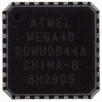
ATMEGA48-20MU Atmel, ATMEGA48-20MU Datasheet - Page 84

ATMEGA48-20MU
Manufacturer Part Number
ATMEGA48-20MU
Description
IC AVR MCU 4K 20MHZ 5V 32-QFN
Manufacturer
Atmel
Series
AVR® ATmegar
Specifications of ATMEGA48-20MU
Core Processor
AVR
Core Size
8-Bit
Speed
20MHz
Connectivity
I²C, SPI, UART/USART
Peripherals
Brown-out Detect/Reset, POR, PWM, WDT
Number Of I /o
23
Program Memory Size
4KB (2K x 16)
Program Memory Type
FLASH
Eeprom Size
256 x 8
Ram Size
512 x 8
Voltage - Supply (vcc/vdd)
2.7 V ~ 5.5 V
Data Converters
A/D 8x10b
Oscillator Type
Internal
Operating Temperature
-40°C ~ 85°C
Package / Case
32-VQFN Exposed Pad, 32-HVQFN, 32-SQFN, 32-DHVQFN
Processor Series
ATMEGA48x
Core
AVR8
Data Bus Width
8 bit
Data Ram Size
512 B
Interface Type
2-Wire/SPI/USART/Serial
Maximum Clock Frequency
20 MHz
Number Of Programmable I/os
23
Number Of Timers
3
Operating Supply Voltage
2.7 V to 5.5 V
Maximum Operating Temperature
+ 85 C
Mounting Style
SMD/SMT
3rd Party Development Tools
EWAVR, EWAVR-BL
Development Tools By Supplier
ATAVRDRAGON, ATSTK500, ATSTK600, ATAVRISP2, ATAVRONEKIT
Minimum Operating Temperature
- 40 C
On-chip Adc
8-ch x 10-bit
Controller Family/series
AVR MEGA
No. Of I/o's
23
Eeprom Memory Size
256Byte
Ram Memory Size
512Byte
Cpu Speed
20MHz
No. Of Timers
3
Rohs Compliant
Yes
Package
32MLF EP
Device Core
AVR
Family Name
ATmega
Maximum Speed
20 MHz
For Use With
ATSTK600-TQFP32 - STK600 SOCKET/ADAPTER 32-TQFPATSTK600-DIP40 - STK600 SOCKET/ADAPTER 40-PDIP770-1007 - ISP 4PORT ATMEL AVR MCU SPI/JTAGATAVRDRAGON - KIT DRAGON 32KB FLASH MEM AVRATAVRISP2 - PROGRAMMER AVR IN SYSTEMATJTAGICE2 - AVR ON-CHIP D-BUG SYSTEM
Lead Free Status / RoHS Status
Lead free / RoHS Compliant
Available stocks
Company
Part Number
Manufacturer
Quantity
Price
Company:
Part Number:
ATMEGA48-20MU
Manufacturer:
ATMEL
Quantity:
18 000
- Current page: 84 of 378
- Download datasheet (8Mb)
• T1/OC0B/PCINT21 – Port D, Bit 5
T1, Timer/Counter1 counter source.
OC0B, Output Compare Match output: The PD5 pin can serve as an external output for the
Timer/Counter0 Compare Match B. The PD5 pin has to be configured as an output (DDD5 set
(one)) to serve this function. The OC0B pin is also the output pin for the PWM mode timer
function.
PCINT21: Pin Change Interrupt source 21. The PD5 pin can serve as an external interrupt
source.
• XCK/T0/PCINT20 – Port D, Bit 4
XCK, USART external clock.
T0, Timer/Counter0 counter source.
PCINT20: Pin Change Interrupt source 20. The PD4 pin can serve as an external interrupt
source.
• INT1/OC2B/PCINT19 – Port D, Bit 3
INT1, External Interrupt source 1: The PD3 pin can serve as an external interrupt source.
OC2B, Output Compare Match output: The PD3 pin can serve as an external output for the
Timer/Counter0 Compare Match B. The PD3 pin has to be configured as an output (DDD3 set
(one)) to serve this function. The OC2B pin is also the output pin for the PWM mode timer
function.
PCINT19: Pin Change Interrupt source 19. The PD3 pin can serve as an external interrupt
source.
• INT0/PCINT18 – Port D, Bit 2
INT0, External Interrupt source 0: The PD2 pin can serve as an external interrupt source.
PCINT18: Pin Change Interrupt source 18. The PD2 pin can serve as an external interrupt
source.
• TXD/PCINT17 – Port D, Bit 1
TXD, Transmit Data (Data output pin for the USART). When the USART Transmitter is enabled,
this pin is configured as an output regardless of the value of DDD1.
PCINT17: Pin Change Interrupt source 17. The PD1 pin can serve as an external interrupt
source.
• RXD/PCINT16 – Port D, Bit 0
RXD, Receive Data (Data input pin for the USART). When the USART Receiver is enabled this
pin is configured as an input regardless of the value of DDD0. When the USART forces this pin
to be an input, the pull-up can still be controlled by the PORTD0 bit.
PCINT16: Pin Change Interrupt source 16. The PD0 pin can serve as an external interrupt
source.
Table 13-10
and
Table 13-11
relate the alternate functions of Port D to the overriding signals
shown in
Figure 13-5 on page
75.
ATmega48/88/168
84
2545S–AVR–07/10
Related parts for ATMEGA48-20MU
Image
Part Number
Description
Manufacturer
Datasheet
Request
R

Part Number:
Description:
IC AVR MCU 4K 5V 20MHZ 32-TQFP
Manufacturer:
Atmel
Datasheet:

Part Number:
Description:
Manufacturer:
Atmel Corporation
Datasheet:

Part Number:
Description:
Manufacturer:
Atmel Corporation
Datasheet:

Part Number:
Description:
IC AVR MCU 4K 20MHZ 5V 32TQFP
Manufacturer:
Atmel
Datasheet:

Part Number:
Description:
IC AVR MCU 4K 20MHZ 5V 28DIP
Manufacturer:
Atmel
Datasheet:

Part Number:
Description:
IC AVR MCU 4K 5V 20MHZ 32-TQFP
Manufacturer:
Atmel
Datasheet:

Part Number:
Description:
IC AVR MCU 4K 5V 20MHZ 32-QFN
Manufacturer:
Atmel
Datasheet:

Part Number:
Description:
IC AVR MCU 4K 5V 20MHZ 32-QFN
Manufacturer:
Atmel
Datasheet:

Part Number:
Description:
IC AVR MCU 4K 5V 20MHZ 28-DIP
Manufacturer:
Atmel
Datasheet:

Part Number:
Description:
IC AVR MCU 4K 5V 20MHZ 28-DIP
Manufacturer:
Atmel
Datasheet:

Part Number:
Description:
IC AVR MCU 4K FLASH 20MHZ 28QFN
Manufacturer:
Atmel
Datasheet:

Part Number:
Description:
MCU AVR 4KB FLASH 20MHZ 32QFN
Manufacturer:
Atmel
Datasheet:


