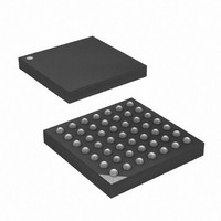
ATXMEGA16A4-CUR Atmel, ATXMEGA16A4-CUR Datasheet - Page 13

ATXMEGA16A4-CUR
Manufacturer Part Number
ATXMEGA16A4-CUR
Description
MCU AVR 16+4KB FLASH 49VFBGA
Manufacturer
Atmel
Series
AVR® XMEGAr
Specifications of ATXMEGA16A4-CUR
Core Processor
AVR
Core Size
8/16-Bit
Speed
32MHz
Connectivity
I²C, IrDA, SPI, UART/USART
Peripherals
Brown-out Detect/Reset, DMA, POR, PWM, WDT
Number Of I /o
34
Program Memory Size
16KB (8K x 16)
Program Memory Type
FLASH
Eeprom Size
1K x 8
Ram Size
2K x 8
Voltage - Supply (vcc/vdd)
1.6 V ~ 3.6 V
Data Converters
A/D 12x12b, D/A 2x12b
Oscillator Type
Internal
Operating Temperature
-40°C ~ 85°C
Package / Case
49-VFBGA
For Use With
ATAVRONEKIT - KIT AVR/AVR32 DEBUGGER/PROGRMMRATSTK600 - DEV KIT FOR AVR/AVR32770-1007 - ISP 4PORT ATMEL AVR MCU SPI/JTAG770-1004 - ISP 4PORT FOR ATMEL AVR MCU SPI
Lead Free Status / RoHS Status
Lead free / RoHS Compliant
Available stocks
Company
Part Number
Manufacturer
Quantity
Price
- Current page: 13 of 445
- Download datasheet (6Mb)
3.12.2
3.13
3.14
3.14.1
3.14.2
8077H–AVR–12/09
Fuse Lock
Register Description
Sequence for execution of protected SPM/LPM
CCP - Configuration Change Protection Register
RAMPD - Extended Direct Addressing Register
Once the correct signature is written by the CPU, interrupts will be ignored for the configuration
change enable period. Any interrupt request (including Non-Maskable Interrupts) during the
CPP period will set the corresponding interrupt flag as normal and the request is kept pending.
After the CPP period any pending interrupts are executed according to their level and priority.
DMA requests are still handled, but do not influence the protected configuration change enable
period. A signature written by the DMA is ignored.
For some system critical features it is possible to program a fuse to disable all changes in the
associated I/O control registers. If this is done, it will not be possible to change the registers from
the user software, and the fuse can only be reprogrammed using an external programmer.
Details on this are described in the data sheet module where this feature is available.
• Bit 7:0 - CCP[7:0] - Configuration Change Protection
The CCP register must be written with the correct signature to enable change of the protected
I/O register or execution of the protected instruction for a maximum of 4 CPU instruction cycles.
All interrupts are ignored during these cycles. After these cycles interrupts automatically handled
again by the CPU, and any pending interrupts will be executed according to their level and prior-
ity. When the Protected I/O register signature is written, CCP[0] will read as one as long as the
protected feature is enabled. Similarly when the Protected SPM/LPM signature is written CCP[1]
will read as one as long as the protected feature is enabled. CCP[7:2] will always be read as
zero.
Table 3-1.
This register is concatenated with the operand for direct addressing (LDS/STS) of the whole
data memory space on devices with more than 64K bytes of data memory. When accessing
Bit
+0x04
Read/Write
Initial Value
1. The application code writes the signature for execution of protected SPM/LPM to the
2. Within 4 instruction cycles, the application code must execute the appropriate instruc-
CCP register.
tion. The protected change is immediately disabled if the CPU performs write
operations to the data memory, or if SLEEP is executed.
Table 3-1 on page 13
Signature
0x9D
0xD8
W
7
0
Modes of CPU Change Protection
W
6
0
Group Configuration
shows the signature for the various modes.
W
5
0
IOREG
SPM
W
4
0
CCP[7:0]
Description
Protected SPM/LPM
Protected IO register
W
3
0
W
2
0
R/W
1
0
XMEGA A
R/W
0
0
CCP
13
Related parts for ATXMEGA16A4-CUR
Image
Part Number
Description
Manufacturer
Datasheet
Request
R

Part Number:
Description:
DEV KIT FOR AVR/AVR32
Manufacturer:
Atmel
Datasheet:

Part Number:
Description:
INTERVAL AND WIPE/WASH WIPER CONTROL IC WITH DELAY
Manufacturer:
ATMEL Corporation
Datasheet:

Part Number:
Description:
Low-Voltage Voice-Switched IC for Hands-Free Operation
Manufacturer:
ATMEL Corporation
Datasheet:

Part Number:
Description:
MONOLITHIC INTEGRATED FEATUREPHONE CIRCUIT
Manufacturer:
ATMEL Corporation
Datasheet:

Part Number:
Description:
AM-FM Receiver IC U4255BM-M
Manufacturer:
ATMEL Corporation
Datasheet:

Part Number:
Description:
Monolithic Integrated Feature Phone Circuit
Manufacturer:
ATMEL Corporation
Datasheet:

Part Number:
Description:
Multistandard Video-IF and Quasi Parallel Sound Processing
Manufacturer:
ATMEL Corporation
Datasheet:

Part Number:
Description:
High-performance EE PLD
Manufacturer:
ATMEL Corporation
Datasheet:

Part Number:
Description:
8-bit Flash Microcontroller
Manufacturer:
ATMEL Corporation
Datasheet:

Part Number:
Description:
2-Wire Serial EEPROM
Manufacturer:
ATMEL Corporation
Datasheet:


