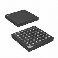
ATXMEGA16A4-CUR Atmel, ATXMEGA16A4-CUR Datasheet - Page 243

ATXMEGA16A4-CUR
Manufacturer Part Number
ATXMEGA16A4-CUR
Description
MCU AVR 16+4KB FLASH 49VFBGA
Manufacturer
Atmel
Series
AVR® XMEGAr
Specifications of ATXMEGA16A4-CUR
Core Processor
AVR
Core Size
8/16-Bit
Speed
32MHz
Connectivity
I²C, IrDA, SPI, UART/USART
Peripherals
Brown-out Detect/Reset, DMA, POR, PWM, WDT
Number Of I /o
34
Program Memory Size
16KB (8K x 16)
Program Memory Type
FLASH
Eeprom Size
1K x 8
Ram Size
2K x 8
Voltage - Supply (vcc/vdd)
1.6 V ~ 3.6 V
Data Converters
A/D 12x12b, D/A 2x12b
Oscillator Type
Internal
Operating Temperature
-40°C ~ 85°C
Package / Case
49-VFBGA
For Use With
ATAVRONEKIT - KIT AVR/AVR32 DEBUGGER/PROGRMMRATSTK600 - DEV KIT FOR AVR/AVR32770-1007 - ISP 4PORT ATMEL AVR MCU SPI/JTAG770-1004 - ISP 4PORT FOR ATMEL AVR MCU SPI
Lead Free Status / RoHS Status
Lead free / RoHS Compliant
Available stocks
Company
Part Number
Manufacturer
Quantity
Price
- Current page: 243 of 445
- Download datasheet (6Mb)
21.7.4
21.7.5
21.8
21.8.1
8077H–AVR–12/09
Asynchronous Data Reception
Disabling the Receiver
Flushing the Receive Buffer
Asynchronous Clock Recovery
A disabling of the Receiver will be immediate. The Receiver buffer will be flushed, and data from
ongoing receptions will be lost.
If the receive buffer has to be flushed during normal operation, read the DATA location until the
Receive Complete Interrupt Flags is cleared.
The USART includes a clock recovery and a data recovery unit for handling asynchronous data
reception. The clock recovery logic is used for synchronizing the incoming asynchronous serial
frames at the RxD pin to the internally generated baud rate clock. The data recovery logic sam-
ples and low pass filters each incoming bit, thereby improving the noise immunity of the
Receiver. The asynchronous reception operational range depends on the accuracy of the inter-
nal baud rate clock, the rate of the incoming frames, and the frame size in number of bits.
The clock recovery logic synchronizes internal clock to the incoming serial frames.
on page 243
rate is 16 times the baud rate for Normal mode, and eight times the baud rate for Double Speed
mode. The horizontal arrows illustrate the synchronization variation due to the sampling pro-
cess. Note the larger time variation when using the Double Speed mode of operation. Samples
denoted zero are samples done when the RxD line is idle, i.e. no communication activity.
Figure 21-6. Start Bit Sampling
When the clock recovery logic detects a high (idle) to low (start) transition on the RxD line, the
start bit detection sequence is initiated. Sample 1 denotes the first zero-sample as shown in the
figure. The clock recovery logic then uses samples 8, 9, and 10 for Normal mode, and samples
4, 5, and 6 for Double Speed mode (indicated with sample numbers inside boxes on the figure)
to decide if a valid start bit is received. If two or more of these three samples have a low level
(the majority wins), the start bit is accepted. The clock recovery logic is synchronized and the
data recovery can begin. If two or more of the three samples have a high level the start bit is
rejected as a noise spike and the Receiver starts looking for the next high to low-transition. The
synchronization process is repeated for each start bit.
(U2X = 0)
(U2X = 1)
Sample
Sample
RxD
0
0
IDLE
illustrates the sampling process of the start bit of an incoming frame. The sample
0
1
1
2
3
2
4
5
3
6
7
4
8
START
9
5
10
11
6
12
13
7
14
15
8
XMEGA A
16
1
1
Figure 21-6
2
BIT 0
3
2
243
Related parts for ATXMEGA16A4-CUR
Image
Part Number
Description
Manufacturer
Datasheet
Request
R

Part Number:
Description:
DEV KIT FOR AVR/AVR32
Manufacturer:
Atmel
Datasheet:

Part Number:
Description:
INTERVAL AND WIPE/WASH WIPER CONTROL IC WITH DELAY
Manufacturer:
ATMEL Corporation
Datasheet:

Part Number:
Description:
Low-Voltage Voice-Switched IC for Hands-Free Operation
Manufacturer:
ATMEL Corporation
Datasheet:

Part Number:
Description:
MONOLITHIC INTEGRATED FEATUREPHONE CIRCUIT
Manufacturer:
ATMEL Corporation
Datasheet:

Part Number:
Description:
AM-FM Receiver IC U4255BM-M
Manufacturer:
ATMEL Corporation
Datasheet:

Part Number:
Description:
Monolithic Integrated Feature Phone Circuit
Manufacturer:
ATMEL Corporation
Datasheet:

Part Number:
Description:
Multistandard Video-IF and Quasi Parallel Sound Processing
Manufacturer:
ATMEL Corporation
Datasheet:

Part Number:
Description:
High-performance EE PLD
Manufacturer:
ATMEL Corporation
Datasheet:

Part Number:
Description:
8-bit Flash Microcontroller
Manufacturer:
ATMEL Corporation
Datasheet:

Part Number:
Description:
2-Wire Serial EEPROM
Manufacturer:
ATMEL Corporation
Datasheet:


