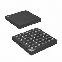
ATXMEGA16A4-CUR Atmel, ATXMEGA16A4-CUR Datasheet - Page 269

ATXMEGA16A4-CUR
Manufacturer Part Number
ATXMEGA16A4-CUR
Description
MCU AVR 16+4KB FLASH 49VFBGA
Manufacturer
Atmel
Series
AVR® XMEGAr
Specifications of ATXMEGA16A4-CUR
Core Processor
AVR
Core Size
8/16-Bit
Speed
32MHz
Connectivity
I²C, IrDA, SPI, UART/USART
Peripherals
Brown-out Detect/Reset, DMA, POR, PWM, WDT
Number Of I /o
34
Program Memory Size
16KB (8K x 16)
Program Memory Type
FLASH
Eeprom Size
1K x 8
Ram Size
2K x 8
Voltage - Supply (vcc/vdd)
1.6 V ~ 3.6 V
Data Converters
A/D 12x12b, D/A 2x12b
Oscillator Type
Internal
Operating Temperature
-40°C ~ 85°C
Package / Case
49-VFBGA
For Use With
ATAVRONEKIT - KIT AVR/AVR32 DEBUGGER/PROGRMMRATSTK600 - DEV KIT FOR AVR/AVR32770-1007 - ISP 4PORT ATMEL AVR MCU SPI/JTAG770-1004 - ISP 4PORT FOR ATMEL AVR MCU SPI
Lead Free Status / RoHS Status
Lead free / RoHS Compliant
Available stocks
Company
Part Number
Manufacturer
Quantity
Price
- Current page: 269 of 445
- Download datasheet (6Mb)
24.3.2
24.3.3
24.4
8077H–AVR–12/09
I/O Pin Configuration
Address Size
Chip Select as Address Lines
The base address associated with each chip select must be on a 4 Kbyte boundary, i.e to
address 0, 4096, 8192 etc.
The address size selects how many bits of the address that should be compared when generat-
ing a chip select. The address size can be anything from 256 bytes to 16M bytes. If the address
space is set to anything larger than 4K bytes, the base address must be on a boundary equal to
the address space. With 1M byte address space for a chip select, the base address must be on
a 0, 1M byte, 2M byte etc. boundary.
If the EBI is configured so that if the address spaces overlap, the internal memory space have
priority, followed by Chip Select 0 (CS0), CS1, CS2 and CS3.
If one or more Chip Select lines are unused, they can in some combinations be used as address
lines instead. This can enable larger external memory or external CS generation. Each column
in
able on unused chip select lines (Ann). Column four shows that all four CS lines are used as
address lines when only CS3 is enabled, and this is for SDRAM configuring.
Figure 24-1. Chip Select and address line combinations
When the EBI is enabled it will override the direction and/or value for the I/O pins where the EBI
lines are placed. The EBI will override the direction and value for the I/O pins where the EBI data
lines are placed. The EBI will only override value, but not direction for the I/O pins where the EBI
address and control lines are placed. These I/O pins must be configured to output when the EBI
is used. I/O pins for unused EBI address and control lines can be used as normal I/O pins or for
other alternate functions on the pins.
For control signals that are active-low, the pin output value should be set to one (high). For con-
trol signals that are active-high, pin output value should be set to zero (low). Address lines does
not requires specific pin output value configuration. The Chip Select lines should have pull-up
resistors to ensure that these are kept high during power-on and reset. If a Chip Select line is
active-high, a pull-down should be used instead of a pull-up.
For more details on I/O pin configuration refer to
Figure 24-1 on page 269
shows enabled chip select lines (CSn), and the address lines avail-
CS3
CS2
CS1
CS0
CS3
CS2
CS1
A16
Section 13. on page
CS3
CS2
A17
A16
A19
A18
A17
A16
129.
XMEGA A
269
Related parts for ATXMEGA16A4-CUR
Image
Part Number
Description
Manufacturer
Datasheet
Request
R

Part Number:
Description:
DEV KIT FOR AVR/AVR32
Manufacturer:
Atmel
Datasheet:

Part Number:
Description:
INTERVAL AND WIPE/WASH WIPER CONTROL IC WITH DELAY
Manufacturer:
ATMEL Corporation
Datasheet:

Part Number:
Description:
Low-Voltage Voice-Switched IC for Hands-Free Operation
Manufacturer:
ATMEL Corporation
Datasheet:

Part Number:
Description:
MONOLITHIC INTEGRATED FEATUREPHONE CIRCUIT
Manufacturer:
ATMEL Corporation
Datasheet:

Part Number:
Description:
AM-FM Receiver IC U4255BM-M
Manufacturer:
ATMEL Corporation
Datasheet:

Part Number:
Description:
Monolithic Integrated Feature Phone Circuit
Manufacturer:
ATMEL Corporation
Datasheet:

Part Number:
Description:
Multistandard Video-IF and Quasi Parallel Sound Processing
Manufacturer:
ATMEL Corporation
Datasheet:

Part Number:
Description:
High-performance EE PLD
Manufacturer:
ATMEL Corporation
Datasheet:

Part Number:
Description:
8-bit Flash Microcontroller
Manufacturer:
ATMEL Corporation
Datasheet:

Part Number:
Description:
2-Wire Serial EEPROM
Manufacturer:
ATMEL Corporation
Datasheet:


