ATTINY84-15MZ Atmel, ATTINY84-15MZ Datasheet - Page 160
ATTINY84-15MZ
Manufacturer Part Number
ATTINY84-15MZ
Description
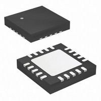
MCU AVR 8K FLASH 15MHZ 20-QFN
Manufacturer
Atmel
Series
AVR® ATtinyr
Specifications of ATTINY84-15MZ
Package / Case
20-QFN Exposed Pad
Voltage - Supply (vcc/vdd)
2.7 V ~ 5.5 V
Operating Temperature
-40°C ~ 125°C
Speed
16MHz
Number Of I /o
12
Eeprom Size
512 x 8
Core Processor
AVR
Program Memory Type
FLASH
Ram Size
512 x 8
Program Memory Size
8KB (8K x 8)
Data Converters
A/D 8x10b
Oscillator Type
Internal
Peripherals
Brown-out Detect/Reset, POR, PWM, WDT
Connectivity
USI
Core Size
8-Bit
Processor Series
ATTINY8x
Core
AVR8
Data Bus Width
8 bit
Data Ram Size
512 B
Interface Type
SPI, UART
Maximum Clock Frequency
16 MHz
Number Of Programmable I/os
12
Number Of Timers
2
Maximum Operating Temperature
+ 85 C
Mounting Style
SMD/SMT
3rd Party Development Tools
EWAVR, EWAVR-BL
Development Tools By Supplier
ATAVRDRAGON, ATSTK500, ATSTK600, ATAVRISP2, ATAVRONEKIT
Minimum Operating Temperature
- 40 C
On-chip Adc
10 bit, 8 Channel
Lead Free Status / RoHS Status
Lead free / RoHS Compliant
Available stocks
Company
Part Number
Manufacturer
Quantity
Price
Company:

Part Number:
ATTINY84-15MZ
Manufacturer:
ATMEL
Quantity:
480
Part Number:
ATTINY84-15MZ
Manufacturer:
ATMEL/爱特梅尔
Quantity:
20 000


20.4.4
20.5
20.5.1
160
Register Description
Atmel ATtiny24/44/84 [Preliminary]
Programming Time for Flash when Using SPM
SPMCSR – Store Program Memory Control and Status Register
Flash corru ptio n ca n e asily b e avoided by fo llowing at lea st one the se d esig n
recommendations:
1. Keep the Atmel
2. Keep the AVR core in power-down sleep mode during periods of low VCC. This will
The calibrated RC Oscillator is used to time Flash accesses.
gramming time for Flash accesses from the CPU.
Table 20-1.
Note:
The Store Program Memory Control and Status Register contains the control bits needed to
control Program memory operations.
• Bits 7..5 – Res: Reserved Bits
These bits are reserved bits in the ATtiny24/44/84 and always read as zero.
• Bit 4 – CTPB: Clear Temporary Page Buffer
If the CTPB bit is written while filling the temporary page buffer, the temporary page buffer will
be cleared and the data will be lost.
• Bit 3 – RFLB: Read Fuse and Lock Bits
An LPM instruction within three cycles after RFLB and SPMEN are set in SPMCSR will read
either the lock bits or the fuse bits (depending on Z0 in the Z-pointer) in the destination regis-
ter. See
• Bit 2 – PGWRT: Page Write
If this bit is written to one at the same time as SPMEN, the next SPM instruction within four
clock cycles executes Page Write, with the data stored in the temporary buffer. The page
address is taken from the high part of the Z-pointer.
Bit
0x37 (0x57)
Read/Write
Initial Value
Flash write (Page Erase, Page Write,
and write Lock bits by SPM)
voltage. This can be done by enabling the internal Brown-out Detector (BOD) if the
operating voltage matches the detection level. If not, an external low V
tion circuit can be used. If a reset occurs while a write operation is in progress, the
write operation will be completed provided the power supply voltage is sufficient.
prevent the CPU from attempting to decode and execute instructions, effectively pro-
tecting SPMCSR and, thus, the flash from unintentional writes.
1. The min and max programming times are per individual operation.
“EEPROM Write Prevents Writing to SPMCSR” on page 159
SPM Programming Time
Symbol
R
7
0
–
®
AVR
®
R
6
0
–
RESET active (low) during periods of insufficient power supply
R
5
–
0
(1)
Min Programming Time
CTPB
R/W
4
0
3.7 ms
RFLB
R/W
3
0
PGWRT
Table 20-1
R/W
2
0
Max Programming Time
PGERS
for details.
R/W
1
0
shows the typical pro-
CC
reset protec-
4.5 ms
SPMEN
R/W
0
0
7701D–AVR–09/10
SPMCSR
Related parts for ATTINY84-15MZ
Image
Part Number
Description
Manufacturer
Datasheet
Request
R

Part Number:
Description:
Manufacturer:
Atmel Corporation
Datasheet:
Part Number:
Description:
Manufacturer:
Atmel Corporation
Datasheet:

Part Number:
Description:
IC MCU AVR 8K FLASH 20MHZ 20-QFN
Manufacturer:
Atmel
Datasheet:

Part Number:
Description:
MCU AVR 8K ISP FLASH 2.7V 14SOIC
Manufacturer:
Atmel
Datasheet:

Part Number:
Description:
IC MCU AVR 8K FLASH 20MHZ 14-DIP
Manufacturer:
Atmel
Datasheet:

Part Number:
Description:
MCU AVR 8KB FLASH 10MHZ 14SOIC
Manufacturer:
Atmel
Datasheet:
Part Number:
Description:
MCU AVR 8KB FLASH 20MHZ 20QFN
Manufacturer:
Atmel
Datasheet:

Part Number:
Description:
DEV KIT FOR AVR/AVR32
Manufacturer:
Atmel
Datasheet:
Part Number:
Description:
INTERVAL AND WIPE/WASH WIPER CONTROL IC WITH DELAY
Manufacturer:
ATMEL Corporation
Datasheet:
Part Number:
Description:
Low-Voltage Voice-Switched IC for Hands-Free Operation
Manufacturer:
ATMEL Corporation
Datasheet:
Part Number:
Description:
MONOLITHIC INTEGRATED FEATUREPHONE CIRCUIT
Manufacturer:
ATMEL Corporation
Datasheet:
Part Number:
Description:
AM-FM Receiver IC U4255BM-M
Manufacturer:
ATMEL Corporation
Datasheet:
Part Number:
Description:
Monolithic Integrated Feature Phone Circuit
Manufacturer:
ATMEL Corporation
Datasheet:
Part Number:
Description:
Multistandard Video-IF and Quasi Parallel Sound Processing
Manufacturer:
ATMEL Corporation
Datasheet: