ATTINY84-15MZ Atmel, ATTINY84-15MZ Datasheet - Page 68
ATTINY84-15MZ
Manufacturer Part Number
ATTINY84-15MZ
Description
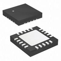
MCU AVR 8K FLASH 15MHZ 20-QFN
Manufacturer
Atmel
Series
AVR® ATtinyr
Specifications of ATTINY84-15MZ
Package / Case
20-QFN Exposed Pad
Voltage - Supply (vcc/vdd)
2.7 V ~ 5.5 V
Operating Temperature
-40°C ~ 125°C
Speed
16MHz
Number Of I /o
12
Eeprom Size
512 x 8
Core Processor
AVR
Program Memory Type
FLASH
Ram Size
512 x 8
Program Memory Size
8KB (8K x 8)
Data Converters
A/D 8x10b
Oscillator Type
Internal
Peripherals
Brown-out Detect/Reset, POR, PWM, WDT
Connectivity
USI
Core Size
8-Bit
Processor Series
ATTINY8x
Core
AVR8
Data Bus Width
8 bit
Data Ram Size
512 B
Interface Type
SPI, UART
Maximum Clock Frequency
16 MHz
Number Of Programmable I/os
12
Number Of Timers
2
Maximum Operating Temperature
+ 85 C
Mounting Style
SMD/SMT
3rd Party Development Tools
EWAVR, EWAVR-BL
Development Tools By Supplier
ATAVRDRAGON, ATSTK500, ATSTK600, ATAVRISP2, ATAVRONEKIT
Minimum Operating Temperature
- 40 C
On-chip Adc
10 bit, 8 Channel
Lead Free Status / RoHS Status
Lead free / RoHS Compliant
Available stocks
Company
Part Number
Manufacturer
Quantity
Price
Company:

Part Number:
ATTINY84-15MZ
Manufacturer:
ATMEL
Quantity:
480
Part Number:
ATTINY84-15MZ
Manufacturer:
ATMEL/爱特梅尔
Quantity:
20 000


68
Atmel ATtiny24/44/84 [Preliminary]
• Port B, Bit 3 – RESET/dW/PCINT11
RESET: External Reset input is active low and enabled by un-programming ("1") the RST-
DISBL fuse. Pull-up is activated and output driver and digital input are deactivated when the
pin is used as the RESET pin.
dW: When the debugWIRE enable (DWEN) fuse is programmed and lock bits are un-pro-
grammed, the debugWIRE system within the target device is activated. The RESET port pin is
configured as a wire-AND (open-drain) bi-directional I/O pin with pull-up enabled and becomes
the communication gateway between target and emulator.
PCINT11: Pin change interrupt source 11. The PB3 pin can serve as an external interrupt
source for pin change interrupt 1.
Table 12-8 on page 68
the overriding signals shown in
Table 12-8.
1.
2.
Signal
Name
PUOE
PUOV
DDOE
DDOV
PVOE
PVOV
PTOE
DIEOE
DIEOV
DI
AIO
RSTDISBL is 1 when the Fuse is “0” (Programmed).
DebugWIRE is enabled when DWEN fuse is programmed and lock bits are un-programmed.
PB3/
PCINT11
RSTDISBL
1
RSTDISBL
DEBUGWIRE_ENABLE
Transmit
RSTDISBL
0
0
RSTDISBL
+ PCINT11 • PCIE1
DEBUGWIRE_ENABLE
• PCINT11 • PCIE1)
dW/PCINT11 Input
Overriding Signals for Alternate Functions in PB3..PB2
RESET/dW/
(1)
(1)
(1)
(1)
+ DEBUGWIRE_ENABLE
+ DEBUGWIRE_ENABLE
+ DEBUGWIRE_ENABLE
+ DEBUGWIRE_ENABLE
and
Table 12-9 on page 69
Figure 12-5 on page
(2)
(2)
• debugWire
+ (RSTDISBL
(2)
(2)
(2)
(2)
(1)
relate the alternate functions of Port B to
61.
PB2/INT0/OC0A/CKOUT/PCINT10
CKOUT
0
CKOUT
1'b1
CKOUT + OC0A enable
CKOUT • System Clock + CKOUT • OC0A
0
PCINT10 • PCIE1 + INT0
PCINT10 • PCIE1 + INT0
INT0/PCINT10 Input
7701D–AVR–09/10
Related parts for ATTINY84-15MZ
Image
Part Number
Description
Manufacturer
Datasheet
Request
R

Part Number:
Description:
Manufacturer:
Atmel Corporation
Datasheet:
Part Number:
Description:
Manufacturer:
Atmel Corporation
Datasheet:

Part Number:
Description:
IC MCU AVR 8K FLASH 20MHZ 20-QFN
Manufacturer:
Atmel
Datasheet:

Part Number:
Description:
MCU AVR 8K ISP FLASH 2.7V 14SOIC
Manufacturer:
Atmel
Datasheet:

Part Number:
Description:
IC MCU AVR 8K FLASH 20MHZ 14-DIP
Manufacturer:
Atmel
Datasheet:

Part Number:
Description:
MCU AVR 8KB FLASH 10MHZ 14SOIC
Manufacturer:
Atmel
Datasheet:
Part Number:
Description:
MCU AVR 8KB FLASH 20MHZ 20QFN
Manufacturer:
Atmel
Datasheet:

Part Number:
Description:
DEV KIT FOR AVR/AVR32
Manufacturer:
Atmel
Datasheet:
Part Number:
Description:
INTERVAL AND WIPE/WASH WIPER CONTROL IC WITH DELAY
Manufacturer:
ATMEL Corporation
Datasheet:
Part Number:
Description:
Low-Voltage Voice-Switched IC for Hands-Free Operation
Manufacturer:
ATMEL Corporation
Datasheet:
Part Number:
Description:
MONOLITHIC INTEGRATED FEATUREPHONE CIRCUIT
Manufacturer:
ATMEL Corporation
Datasheet:
Part Number:
Description:
AM-FM Receiver IC U4255BM-M
Manufacturer:
ATMEL Corporation
Datasheet:
Part Number:
Description:
Monolithic Integrated Feature Phone Circuit
Manufacturer:
ATMEL Corporation
Datasheet:
Part Number:
Description:
Multistandard Video-IF and Quasi Parallel Sound Processing
Manufacturer:
ATMEL Corporation
Datasheet: