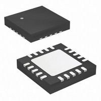
ATTINY84-15MZ Atmel, ATTINY84-15MZ Datasheet - Page 83
ATTINY84-15MZ
Manufacturer Part Number
ATTINY84-15MZ
Description
MCU AVR 8K FLASH 15MHZ 20-QFN
Manufacturer
Atmel
Series
AVR® ATtinyr
Specifications of ATTINY84-15MZ
Package / Case
20-QFN Exposed Pad
Voltage - Supply (vcc/vdd)
2.7 V ~ 5.5 V
Operating Temperature
-40°C ~ 125°C
Speed
16MHz
Number Of I /o
12
Eeprom Size
512 x 8
Core Processor
AVR
Program Memory Type
FLASH
Ram Size
512 x 8
Program Memory Size
8KB (8K x 8)
Data Converters
A/D 8x10b
Oscillator Type
Internal
Peripherals
Brown-out Detect/Reset, POR, PWM, WDT
Connectivity
USI
Core Size
8-Bit
Processor Series
ATTINY8x
Core
AVR8
Data Bus Width
8 bit
Data Ram Size
512 B
Interface Type
SPI, UART
Maximum Clock Frequency
16 MHz
Number Of Programmable I/os
12
Number Of Timers
2
Maximum Operating Temperature
+ 85 C
Mounting Style
SMD/SMT
3rd Party Development Tools
EWAVR, EWAVR-BL
Development Tools By Supplier
ATAVRDRAGON, ATSTK500, ATSTK600, ATAVRISP2, ATAVRONEKIT
Minimum Operating Temperature
- 40 C
On-chip Adc
10 bit, 8 Channel
Lead Free Status / RoHS Status
Lead free / RoHS Compliant
Available stocks
Company
Part Number
Manufacturer
Quantity
Price
Company:

Part Number:
ATTINY84-15MZ
Manufacturer:
ATMEL
Quantity:
480
Part Number:
ATTINY84-15MZ
Manufacturer:
ATMEL/爱特梅尔
Quantity:
20 000


13.9
13.9.1
7701D–AVR–09/10
Register Description
TCCR0A – Timer/Counter Control Register A
• Bits 7:6 – COM0A1:0: Compare Match Output A Mode
These bits control the output compare pin (OC0A) behavior. If one or both of the COM0A1:0
bits are set, the OC0A output overrides the normal port functionality of the I/O pin it is con-
nected to. However, note that the data direction register (DDR) bit corresponding to the OC0A
pin must be set in order to enable the output driver.
When OC0A is connected to the pin, the function of the COM0A1:0 bits depends on the
WGM02:0 bit setting.
WGM02:0 bits are set to a normal or CTC mode (non-PWM).
Table 13-2.
Table 13-3 on page 83
to fast PWM mode.
Table 13-3.
Note:
Bit
0x30 (0x50)
Read/Write
Initial Value
COM01
COM01
0
0
1
1
0
0
1
1
1. A special case occurs when OCR0A equals TOP and COM0A1 is set. In this case, the Com-
pare Match is ignored, but the set or clear is done at BOTTOM. See
page 77
COM0A1
Compare Output Mode, non-PWM Mode
Compare Output Mode, Fast PWM Mode
R/W
7
0
COM00
COM00
for more details.
0
1
0
1
0
1
0
1
Table 13-2 on page 83
shows the COM0A1:0 bit functionality when the WGM01:0 bits are set
COM0A0
R/W
6
0
Atmel ATtiny24/44/84 [Preliminary]
Description
Normal port operation, OC0A disconnected.
WGM02 = 0: Normal Port Operation, OC0A Disconnected.
WGM02 = 1: Toggle OC0A on Compare Match.
Clear OC0A on Compare Match, set OC0A at BOTTOM
(non-inverting mode)
Set OC0A on Compare Match, clear OC0A at BOTTOM
(inverting mode)
Description
Normal port operation, OC0A disconnected.
Toggle OC0A on Compare Match
Clear OC0A on Compare Match
Set OC0A on Compare Match
COM0B1
R/W
5
0
COM0B0
R/W
4
0
shows the COM0A1:0 bit functionality when the
R
3
–
0
(1)
R
2
0
–
WGM01
R/W
1
0
“Fast PWM Mode” on
WGM00
R/W
0
0
TCCR0A
83
Related parts for ATTINY84-15MZ
Image
Part Number
Description
Manufacturer
Datasheet
Request
R

Part Number:
Description:
Manufacturer:
Atmel Corporation
Datasheet:
Part Number:
Description:
Manufacturer:
Atmel Corporation
Datasheet:

Part Number:
Description:
IC MCU AVR 8K FLASH 20MHZ 20-QFN
Manufacturer:
Atmel
Datasheet:

Part Number:
Description:
MCU AVR 8K ISP FLASH 2.7V 14SOIC
Manufacturer:
Atmel
Datasheet:

Part Number:
Description:
IC MCU AVR 8K FLASH 20MHZ 14-DIP
Manufacturer:
Atmel
Datasheet:

Part Number:
Description:
MCU AVR 8KB FLASH 10MHZ 14SOIC
Manufacturer:
Atmel
Datasheet:
Part Number:
Description:
MCU AVR 8KB FLASH 20MHZ 20QFN
Manufacturer:
Atmel
Datasheet:

Part Number:
Description:
DEV KIT FOR AVR/AVR32
Manufacturer:
Atmel
Datasheet:
Part Number:
Description:
INTERVAL AND WIPE/WASH WIPER CONTROL IC WITH DELAY
Manufacturer:
ATMEL Corporation
Datasheet:
Part Number:
Description:
Low-Voltage Voice-Switched IC for Hands-Free Operation
Manufacturer:
ATMEL Corporation
Datasheet:
Part Number:
Description:
MONOLITHIC INTEGRATED FEATUREPHONE CIRCUIT
Manufacturer:
ATMEL Corporation
Datasheet:
Part Number:
Description:
AM-FM Receiver IC U4255BM-M
Manufacturer:
ATMEL Corporation
Datasheet:
Part Number:
Description:
Monolithic Integrated Feature Phone Circuit
Manufacturer:
ATMEL Corporation
Datasheet:
Part Number:
Description:
Multistandard Video-IF and Quasi Parallel Sound Processing
Manufacturer:
ATMEL Corporation
Datasheet: