ATTINY84-15MZ Atmel, ATTINY84-15MZ Datasheet - Page 63
ATTINY84-15MZ
Manufacturer Part Number
ATTINY84-15MZ
Description
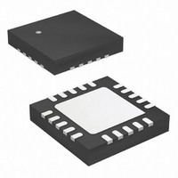
MCU AVR 8K FLASH 15MHZ 20-QFN
Manufacturer
Atmel
Series
AVR® ATtinyr
Specifications of ATTINY84-15MZ
Package / Case
20-QFN Exposed Pad
Voltage - Supply (vcc/vdd)
2.7 V ~ 5.5 V
Operating Temperature
-40°C ~ 125°C
Speed
16MHz
Number Of I /o
12
Eeprom Size
512 x 8
Core Processor
AVR
Program Memory Type
FLASH
Ram Size
512 x 8
Program Memory Size
8KB (8K x 8)
Data Converters
A/D 8x10b
Oscillator Type
Internal
Peripherals
Brown-out Detect/Reset, POR, PWM, WDT
Connectivity
USI
Core Size
8-Bit
Processor Series
ATTINY8x
Core
AVR8
Data Bus Width
8 bit
Data Ram Size
512 B
Interface Type
SPI, UART
Maximum Clock Frequency
16 MHz
Number Of Programmable I/os
12
Number Of Timers
2
Maximum Operating Temperature
+ 85 C
Mounting Style
SMD/SMT
3rd Party Development Tools
EWAVR, EWAVR-BL
Development Tools By Supplier
ATAVRDRAGON, ATSTK500, ATSTK600, ATAVRISP2, ATAVRONEKIT
Minimum Operating Temperature
- 40 C
On-chip Adc
10 bit, 8 Channel
Lead Free Status / RoHS Status
Lead free / RoHS Compliant
Available stocks
Company
Part Number
Manufacturer
Quantity
Price
Company:

Part Number:
ATTINY84-15MZ
Manufacturer:
ATMEL
Quantity:
480
Part Number:
ATTINY84-15MZ
Manufacturer:
ATMEL/爱特梅尔
Quantity:
20 000


12.3.1
7701D–AVR–09/10
Alternate Functions of Port A
The Port A pins with alternate function are shown in
Table 12-3.
• Port A, Bit 0 – ADC0/AREF/PCINT0
ADC0: Analog to Digital Converter, Channel 0
AREF: External Analog Reference for ADC. Pullup and output driver are disabled on PA0
when the pin is used as an external reference or Internal Voltage Reference with external
capacitor at the AREF pin by setting (one) the bit REFS0 in the ADC Multiplexer Selection
Register (ADMUX).
PCINT0: Pin Change Interrupt source 0. The PA0 pin can serve as an external interrupt
source for pin change interrupt 0.
Port Pin
PA0
PA1
PA2
PA3
PA4
PA5
PA6
PA7
Port A Pins Alternate Functions
Atmel ATtiny24/44/84 [Preliminary]
Alternate Function
ADC0: ADC input channel 0.
AREF: External analog reference.
PCINT0: Pin change interrupt 0 source 0.
ADC1:
AIN0:
PCINT1:Pin change interrupt 0 source 1.
ADC2:
AIN1:
PCINT2: Pin change interrupt 0 source 2.
T0:
PCINT3: Pin change interrupt 0 source 3.
ADC4:
USCK: USI Clock three wire mode.
SCL:
T1:
PCINT4: Pin change interrupt 0 source 4.
ADC5:
DO:
OC1B: Timer/Counter1 Compare Match B output.
PCINT5: Pin change interrupt 0 source 5.
ADC6:
DI:
SDA:
OC1A: Timer/Counter1 Compare Match A output.
PCINT6: Pin change interrupt 0 source 6.
ADC7:
OC0B: Timer/Counter0 Compare Match B output.
ICP1:
PCINT7: Pin change interrupt 0 source 7.
ADC3: ADC input channel 3.
ADC input channel 1.
Analog Comparator Positive Input.
ADC input channel 2.
Analog Comparator Negative Input.
Timer/Counter0 counter source.
ADC input channel 4.
USI Clock two wire mode.
Timer/Counter1 counter source.
ADC input channel 5.
USI Data Output three wire mode.
ADC input channel 6.
USI Data Input three wire mode.
USI Data Input two wire mode.
ADC input channel 7.
Timer/Counter1 Input Capture Pin.
.
Table 12-7 on page
67.
63
Related parts for ATTINY84-15MZ
Image
Part Number
Description
Manufacturer
Datasheet
Request
R

Part Number:
Description:
Manufacturer:
Atmel Corporation
Datasheet:
Part Number:
Description:
Manufacturer:
Atmel Corporation
Datasheet:

Part Number:
Description:
IC MCU AVR 8K FLASH 20MHZ 20-QFN
Manufacturer:
Atmel
Datasheet:

Part Number:
Description:
MCU AVR 8K ISP FLASH 2.7V 14SOIC
Manufacturer:
Atmel
Datasheet:

Part Number:
Description:
IC MCU AVR 8K FLASH 20MHZ 14-DIP
Manufacturer:
Atmel
Datasheet:

Part Number:
Description:
MCU AVR 8KB FLASH 10MHZ 14SOIC
Manufacturer:
Atmel
Datasheet:
Part Number:
Description:
MCU AVR 8KB FLASH 20MHZ 20QFN
Manufacturer:
Atmel
Datasheet:

Part Number:
Description:
DEV KIT FOR AVR/AVR32
Manufacturer:
Atmel
Datasheet:
Part Number:
Description:
INTERVAL AND WIPE/WASH WIPER CONTROL IC WITH DELAY
Manufacturer:
ATMEL Corporation
Datasheet:
Part Number:
Description:
Low-Voltage Voice-Switched IC for Hands-Free Operation
Manufacturer:
ATMEL Corporation
Datasheet:
Part Number:
Description:
MONOLITHIC INTEGRATED FEATUREPHONE CIRCUIT
Manufacturer:
ATMEL Corporation
Datasheet:
Part Number:
Description:
AM-FM Receiver IC U4255BM-M
Manufacturer:
ATMEL Corporation
Datasheet:
Part Number:
Description:
Monolithic Integrated Feature Phone Circuit
Manufacturer:
ATMEL Corporation
Datasheet:
Part Number:
Description:
Multistandard Video-IF and Quasi Parallel Sound Processing
Manufacturer:
ATMEL Corporation
Datasheet: