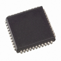
AT89C51CC01UA-SLSUM Atmel, AT89C51CC01UA-SLSUM Datasheet - Page 105

AT89C51CC01UA-SLSUM
Manufacturer Part Number
AT89C51CC01UA-SLSUM
Description
IC 8051 MCU FLASH 32K 44-PLCC
Manufacturer
Atmel
Series
AT89C CANr
Datasheet
1.T89C51CC01CA-7CTIM.pdf
(167 pages)
Specifications of AT89C51CC01UA-SLSUM
Core Processor
8051
Core Size
8-Bit
Speed
40MHz
Connectivity
CAN, UART/USART
Peripherals
POR, PWM, WDT
Number Of I /o
34
Program Memory Size
32KB (32K x 8)
Program Memory Type
FLASH
Eeprom Size
2K x 8
Ram Size
1.25K x 8
Voltage - Supply (vcc/vdd)
3 V ~ 5.5 V
Data Converters
A/D 8x10b
Oscillator Type
External
Operating Temperature
-40°C ~ 85°C
Package / Case
44-PLCC
Package
44PLCC
Device Core
8051
Family Name
89C
Maximum Speed
40 MHz
Operating Supply Voltage
3.3|5 V
Data Bus Width
8 Bit
Number Of Programmable I/os
34
Interface Type
CAN/UART
On-chip Adc
8-chx10-bit
Number Of Timers
3
Processor Series
AT89x
Core
8051
Data Ram Size
1280 B
Maximum Clock Frequency
40 MHz
Maximum Operating Temperature
+ 85 C
Mounting Style
SMD/SMT
3rd Party Development Tools
PK51, CA51, A51, ULINK2
Development Tools By Supplier
CANADAPT28
Minimum Operating Temperature
- 40 C
Cpu Family
AT89
Device Core Size
8b
Frequency (max)
40MHz
Total Internal Ram Size
1.25KB
# I/os (max)
34
Number Of Timers - General Purpose
3
Operating Supply Voltage (typ)
3.3/5V
Operating Supply Voltage (max)
5.5V
Operating Supply Voltage (min)
3V
Instruction Set Architecture
CISC
Operating Temp Range
-40C to 85C
Operating Temperature Classification
Industrial
Mounting
Surface Mount
Pin Count
44
Package Type
PLCC
For Use With
AT89OCD-01 - USB EMULATOR FOR AT8XC51 MCU
Lead Free Status / RoHS Status
Lead free / RoHS Compliant
Other names
AT89C51CC01UASLSUM
Available stocks
Company
Part Number
Manufacturer
Quantity
Price
Company:
Part Number:
AT89C51CC01UA-SLSUM
Manufacturer:
ATMEL
Quantity:
678
4129N–CAN–03/08
Table 72. CANBT3 Register
CANBT3 (S:B6h)
CAN Bit Timing Registers 3
Note:
No default value after reset.
Number
Bit
6-4
3-1
7
-
7
0
The CAN controller bit timing registers must be accessed only if the CAN controller is dis-
abled with the ENA bit of the CANGCON register set to 0.
See Figure 48.
Bit Mnemonic Description
PHS2 2
PHS2 2:0
PHS1 2:0
SMP
6
-
PHS2 1
Reserved
The value read from this bit is indeterminate. Do not set this bit.
Phase Segment 2
This phase is used to compensate for phase edge errors. This segment can
be shortened by the re-synchronization jump width.
Phase segment 2 is the maximum of Phase segment1 and the Information
Processing Time (= 2TQ).
Phase Segment 1
This phase is used to compensate for phase edge errors. This segment can
be lengthened by the re-synchronization jump width.
Sample Type
0 - once, at the sample point.
1 - three times, the threefold sampling of the bus is the sample point and twice
over a distance of a 1/2 period of the Tscl. The result corresponds to the
majority decision of the three values.
5
PHS2 0
4
Tphs2 = Tscl x (PHS2[2..0] + 1)
Tphs1 = Tscl x (PHS1[2..0] + 1)
PHS1 2
3
PHS1 1
2
PHS1 0
1
SMP
0
105


