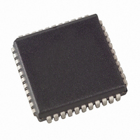
AT89C51CC01UA-SLSUM Atmel, AT89C51CC01UA-SLSUM Datasheet - Page 6

AT89C51CC01UA-SLSUM
Manufacturer Part Number
AT89C51CC01UA-SLSUM
Description
IC 8051 MCU FLASH 32K 44-PLCC
Manufacturer
Atmel
Series
AT89C CANr
Datasheet
1.T89C51CC01CA-7CTIM.pdf
(167 pages)
Specifications of AT89C51CC01UA-SLSUM
Core Processor
8051
Core Size
8-Bit
Speed
40MHz
Connectivity
CAN, UART/USART
Peripherals
POR, PWM, WDT
Number Of I /o
34
Program Memory Size
32KB (32K x 8)
Program Memory Type
FLASH
Eeprom Size
2K x 8
Ram Size
1.25K x 8
Voltage - Supply (vcc/vdd)
3 V ~ 5.5 V
Data Converters
A/D 8x10b
Oscillator Type
External
Operating Temperature
-40°C ~ 85°C
Package / Case
44-PLCC
Package
44PLCC
Device Core
8051
Family Name
89C
Maximum Speed
40 MHz
Operating Supply Voltage
3.3|5 V
Data Bus Width
8 Bit
Number Of Programmable I/os
34
Interface Type
CAN/UART
On-chip Adc
8-chx10-bit
Number Of Timers
3
Processor Series
AT89x
Core
8051
Data Ram Size
1280 B
Maximum Clock Frequency
40 MHz
Maximum Operating Temperature
+ 85 C
Mounting Style
SMD/SMT
3rd Party Development Tools
PK51, CA51, A51, ULINK2
Development Tools By Supplier
CANADAPT28
Minimum Operating Temperature
- 40 C
Cpu Family
AT89
Device Core Size
8b
Frequency (max)
40MHz
Total Internal Ram Size
1.25KB
# I/os (max)
34
Number Of Timers - General Purpose
3
Operating Supply Voltage (typ)
3.3/5V
Operating Supply Voltage (max)
5.5V
Operating Supply Voltage (min)
3V
Instruction Set Architecture
CISC
Operating Temp Range
-40C to 85C
Operating Temperature Classification
Industrial
Mounting
Surface Mount
Pin Count
44
Package Type
PLCC
For Use With
AT89OCD-01 - USB EMULATOR FOR AT8XC51 MCU
Lead Free Status / RoHS Status
Lead free / RoHS Compliant
Other names
AT89C51CC01UASLSUM
Available stocks
Company
Part Number
Manufacturer
Quantity
Price
Company:
Part Number:
AT89C51CC01UA-SLSUM
Manufacturer:
ATMEL
Quantity:
678
Quasi-Bidirectional Port
Operation
6
A/T89C51CC01
Table 1. Read-Modify-Write Instructions
It is not obvious the last three instructions in this list are Read-Modify-Write instructions.
These instructions read the port (all 8 bits), modify the specifically addressed bit and
write the new byte back to the latch. These Read-Modify-Write instructions are directed
to the latch rather than the pin in order to avoid possible misinterpretation of voltage
(and therefore, logic) levels at the pin. For example, a Port bit used to drive the base of
an external bipolar transistor can not rise above the transistor’s base-emitter junction
voltage (a value lower than VIL). With a logic one written to the bit, attempts by the CPU
to read the Port at the pin are misinterpreted as logic zero. A read of the latch rather
than the pins returns the correct logic-one value.
Port 1, Port 2, Port 3 and Port 4 have fixed internal pull-ups and are referred to as
"quasi-bidirectional" Ports. When configured as an input, the pin impedance appears as
logic one and sources current in response to an external logic zero condition. Port 0 is a
"true bidirectional" pin. The pins float when configured as input. Resets write logic one to
all Port latches. If logical zero is subsequently written to a Port latch, it can be returned
to input conditions by a logical one written to the latch.
Note:
Logical zero-to-one transitions in Port 1, Port 2, Port 3 and Port 4 use an additional pull-
up (p1) to aid this logic transition (see Figure 4.). This increases switch speed. This
extra pull-up sources 100 times normal internal circuit current during 2 oscillator clock
periods. The internal pull-ups are field-effect transistors rather than linear resistors. Pull-
ups consist of three p-channel FET (pFET) devices. A pFET is on when the gate senses
logical zero and off when the gate senses logical one. pFET #1 is turned on for two
oscillator periods immediately after a zero-to-one transition in the Port latch. A logical
one at the Port pin turns on pFET #3 (a weak pull-up) through the inverter. This inverter
and pFET pair form a latch to drive logical one. pFET #2 is a very weak pull-up switched
on whenever the associated nFET is switched off. This is traditional CMOS switch con-
vention. Current strengths are 1/10 that of pFET #3.
MOV Px.y, C
Instruction
CLR Px.y
SET Px.y
DJNZ
DEC
ANL
ORL
XRL
CPL
JBC
INC
Port latch values change near the end of Read-Modify-Write instruction cycles. Output
buffers (and therefore the pin state) update early in the instruction after Read-Modify-
Write instruction cycle.
Description
logical AND
logical OR
logical EX-OR
jump if bit = 1 and clear bit
complement bit
increment
decrement
decrement and jump if not zero
move carry bit to bit y of Port x
clear bit y of Port x
set bit y of Port x
Example
ANL P1, A
ORL P2, A
XRL P3, A
JBC P1.1, LABEL
CPL P3.0
INC P2
DEC P2
DJNZ P3, LABEL
MOV P1.5, C
CLR P2.4
SET P3.3
4129N–CAN–03/08


