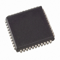
AT89C51CC01UA-SLSUM Atmel, AT89C51CC01UA-SLSUM Datasheet - Page 132

AT89C51CC01UA-SLSUM
Manufacturer Part Number
AT89C51CC01UA-SLSUM
Description
IC 8051 MCU FLASH 32K 44-PLCC
Manufacturer
Atmel
Series
AT89C CANr
Datasheet
1.T89C51CC01CA-7CTIM.pdf
(167 pages)
Specifications of AT89C51CC01UA-SLSUM
Core Processor
8051
Core Size
8-Bit
Speed
40MHz
Connectivity
CAN, UART/USART
Peripherals
POR, PWM, WDT
Number Of I /o
34
Program Memory Size
32KB (32K x 8)
Program Memory Type
FLASH
Eeprom Size
2K x 8
Ram Size
1.25K x 8
Voltage - Supply (vcc/vdd)
3 V ~ 5.5 V
Data Converters
A/D 8x10b
Oscillator Type
External
Operating Temperature
-40°C ~ 85°C
Package / Case
44-PLCC
Package
44PLCC
Device Core
8051
Family Name
89C
Maximum Speed
40 MHz
Operating Supply Voltage
3.3|5 V
Data Bus Width
8 Bit
Number Of Programmable I/os
34
Interface Type
CAN/UART
On-chip Adc
8-chx10-bit
Number Of Timers
3
Processor Series
AT89x
Core
8051
Data Ram Size
1280 B
Maximum Clock Frequency
40 MHz
Maximum Operating Temperature
+ 85 C
Mounting Style
SMD/SMT
3rd Party Development Tools
PK51, CA51, A51, ULINK2
Development Tools By Supplier
CANADAPT28
Minimum Operating Temperature
- 40 C
Cpu Family
AT89
Device Core Size
8b
Frequency (max)
40MHz
Total Internal Ram Size
1.25KB
# I/os (max)
34
Number Of Timers - General Purpose
3
Operating Supply Voltage (typ)
3.3/5V
Operating Supply Voltage (max)
5.5V
Operating Supply Voltage (min)
3V
Instruction Set Architecture
CISC
Operating Temp Range
-40C to 85C
Operating Temperature Classification
Industrial
Mounting
Surface Mount
Pin Count
44
Package Type
PLCC
For Use With
AT89OCD-01 - USB EMULATOR FOR AT8XC51 MCU
Lead Free Status / RoHS Status
Lead free / RoHS Compliant
Other names
AT89C51CC01UASLSUM
Available stocks
Company
Part Number
Manufacturer
Quantity
Price
Company:
Part Number:
AT89C51CC01UA-SLSUM
Manufacturer:
ATMEL
Quantity:
678
Figure 61. A/D Converter clock
ADC Standby Mode
IT ADC Management
Routines examples
132
A/T89C51CC01
CPU Core Clock Symbol
CLOCK
CPU
When the ADC is not used, it is possible to set it in standby mode by clearing bit ADEN
in ADCON register. In this mode its power dissipation is reduced.
An interrupt end-of-conversion will occurs when the bit ADEOC is activated and the bit
EADC is set. For re-arming the interrupt the bit ADEOC must be cleared by software.
Figure 62. ADC Interrupt Structure
1. Configure P1.2 and P1.3 in ADC channels
2. Start a standard conversion
3. Start a precision conversion (need interrupt ADC)
// configure channel P1.2 and P1.3 for ADC
// Enable the ADC
// The variable "channel" contains the channel to convert
// The variable "value_converted" is an unsigned int
// Clear the field SCH[2:0]
// Select channel
// Start conversion in standard mode
// Wait flag End of conversion
// Clear the End of conversion flag
// read the value
// The variable "channel" contains the channel to convert
// Enable ADC
ADCF = 0Ch
ADCON = 20h
ADCON and = F8h
ADCON | = channel
ADCON | = 08h
while((ADCON and 01h)! = 01h)
ADCON and = EFh
value_converted = (ADDH << 2)+(ADDL)
EADC = 1
÷
2
ADEOC
ADCON.2
Prescaler ADCLK
EADC
IEN1.1
ADC Clock
Converter
ADCI
A/D
4129N–CAN–03/08


