AT32UC3B0128-A2UT Atmel, AT32UC3B0128-A2UT Datasheet - Page 279
AT32UC3B0128-A2UT
Manufacturer Part Number
AT32UC3B0128-A2UT
Description
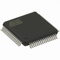
IC MCU AVR32 128KB FLASH 64-TQFP
Manufacturer
Atmel
Series
AVR®32 UC3r
Specifications of AT32UC3B0128-A2UT
Core Processor
AVR
Core Size
32-Bit
Speed
60MHz
Connectivity
I²C, IrDA, SPI, SSC, UART/USART, USB
Peripherals
Brown-out Detect/Reset, DMA, POR, PWM, WDT
Number Of I /o
44
Program Memory Size
128KB (128K x 8)
Program Memory Type
FLASH
Ram Size
32K x 8
Voltage - Supply (vcc/vdd)
1.65 V ~ 1.95 V
Data Converters
A/D 8x10b
Oscillator Type
Internal
Operating Temperature
-40°C ~ 85°C
Package / Case
64-TQFP, 64-VQFP
Processor Series
AT32UC3x
Core
AVR32
Data Bus Width
32 bit
Data Ram Size
32 KB
Interface Type
2-Wire, SPI, USART
Maximum Clock Frequency
60 MHz
Number Of Programmable I/os
44
Number Of Timers
3
Maximum Operating Temperature
+ 85 C
Mounting Style
SMD/SMT
3rd Party Development Tools
EWAVR32, EWAVR32-BL
Development Tools By Supplier
ATAVRDRAGON, ATSTK500, ATSTK600, ATAVRISP2, ATAVRONEKIT, ATEXTWIFI, ATEVK1101
Minimum Operating Temperature
- 40 C
On-chip Adc
10 bit, 8 Channel
Package
64TQFP
Device Core
AVR32
Family Name
AT32
Maximum Speed
60 MHz
Operating Supply Voltage
1.8|3.3 V
For Use With
ATAVRONEKIT - KIT AVR/AVR32 DEBUGGER/PROGRMMR770-1008 - ISP 4PORT ATMEL AVR32 MCU SPIATSTK600-TQFP64-2 - STK600 SOCKET/ADAPTER FOR 64-TQFATEVK1101 - KIT DEV/EVAL FOR AVR32 AT32UC3B
Lead Free Status / RoHS Status
Lead free / RoHS Compliant
Eeprom Size
-
Lead Free Status / Rohs Status
Details
Available stocks
Company
Part Number
Manufacturer
Quantity
Price
Company:

Part Number:
AT32UC3B0128-A2UT
Manufacturer:
XILINX
Quantity:
150


• START: Receive Start Selection
• CKG: Receive Clock Gating Selection
• CKI: Receive Clock Inversion
• CKO: Receive Clock Output Mode Selection
• CKS: Receive Clock Selection
32059K–03/2011
START
Others
Others
CKG
CKS
CKO
0
1
2
3
0
1
2
3
4
5
6
7
8
0
1
2
3
0
1
2
CKI affects only the receive clock and not the output clock signal.
1: The data inputs (Data and Frame Sync signals) are sampled on receive clock rising edge. The Frame Sync signal output is
shifted out on receive clock falling edge.
0: The data inputs (Data and Frame Sync signals) are sampled on receive clock falling edge. The Frame Sync signal output is
shifted out on receive clock rising edge.
Selected Receive Clock
Divided clock
TX_CLOCK clock signal
RX_CLOCK pin
Reserved
Continuous, as soon as the receiver is enabled, and immediately after the end of
transfer of the previous data.
Transmit start
Detection of a low level on RX_FRAME_SYNC signal
Detection of a high level on RX_FRAME_SYNC signal
Detection of a falling edge on RX_FRAME_SYNC signal
Detection of a rising edge on RX_FRAME_SYNC signal
Detection of any level change on RX_FRAME_SYNC signal
Detection of any edge on RX_FRAME_SYNC signal
Compare 0
Reserved
None, continuous clock
Receive Clock enabled only if RX_FRAME_SYNC is low
Receive Clock enabled only if RX_FRAME_SYNC is high
Reserved
Receive Clock Output Mode
None
Continuous receive clock
Receive clock only during data transfers
Reserved
Receive Start
Receive Clock Gating
RX_CLOCK pin
Input-only
Output
Output
AT32UC3B
279
Related parts for AT32UC3B0128-A2UT
Image
Part Number
Description
Manufacturer
Datasheet
Request
R

Part Number:
Description:
DEV KIT FOR AVR/AVR32
Manufacturer:
Atmel
Datasheet:

Part Number:
Description:
INTERVAL AND WIPE/WASH WIPER CONTROL IC WITH DELAY
Manufacturer:
ATMEL Corporation
Datasheet:
Part Number:
Description:
Low-Voltage Voice-Switched IC for Hands-Free Operation
Manufacturer:
ATMEL Corporation
Datasheet:
Part Number:
Description:
MONOLITHIC INTEGRATED FEATUREPHONE CIRCUIT
Manufacturer:
ATMEL Corporation
Datasheet:
Part Number:
Description:
AM-FM Receiver IC U4255BM-M
Manufacturer:
ATMEL Corporation
Datasheet:
Part Number:
Description:
Monolithic Integrated Feature Phone Circuit
Manufacturer:
ATMEL Corporation
Datasheet:
Part Number:
Description:
Multistandard Video-IF and Quasi Parallel Sound Processing
Manufacturer:
ATMEL Corporation
Datasheet:
Part Number:
Description:
High-performance EE PLD
Manufacturer:
ATMEL Corporation
Datasheet:
Part Number:
Description:
8-bit Flash Microcontroller
Manufacturer:
ATMEL Corporation
Datasheet:
Part Number:
Description:
2-Wire Serial EEPROM
Manufacturer:
ATMEL Corporation
Datasheet: