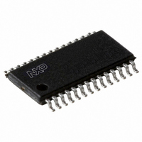
P89LPC931A1FDH,512 NXP Semiconductors, P89LPC931A1FDH,512 Datasheet - Page 24

P89LPC931A1FDH,512
Manufacturer Part Number
P89LPC931A1FDH,512
Description
IC 80C51 MCU FLASH 8K 28-TSSOP
Manufacturer
NXP Semiconductors
Series
LPC900r
Datasheet
1.P89LPC9301FDH512.pdf
(66 pages)
Specifications of P89LPC931A1FDH,512
Program Memory Type
FLASH
Program Memory Size
8KB (8K x 8)
Package / Case
28-TSSOP
Core Processor
8051
Core Size
8-Bit
Speed
18MHz
Connectivity
I²C, SPI, UART/USART
Peripherals
Brown-out Detect/Reset, POR, PWM, WDT
Number Of I /o
26
Ram Size
256 x 8
Voltage - Supply (vcc/vdd)
2.4 V ~ 3.6 V
Oscillator Type
Internal
Operating Temperature
-40°C ~ 85°C
Processor Series
P89LPC
Core
80C51
Data Bus Width
8 bit
Data Ram Size
256 B
Interface Type
I2C, SPI, UART
Maximum Clock Frequency
18 MHz
Number Of Programmable I/os
23
Number Of Timers
3
Operating Supply Voltage
2.4 V to 3.6 V
Maximum Operating Temperature
+ 85 C
Mounting Style
SMD/SMT
3rd Party Development Tools
PK51, CA51, A51, ULINK2
Minimum Operating Temperature
- 40 C
Lead Free Status / RoHS Status
Lead free / RoHS Compliant
For Use With
568-1758 - BOARD EVAL FOR LPC93X MCU FAMILY
Eeprom Size
-
Data Converters
-
Lead Free Status / Rohs Status
Lead free / RoHS Compliant
Other names
935288634512
NXP Semiconductors
P89LPC9301_931A1
Product data sheet
7.16.1.3 Input-only configuration
7.16.1.4 Push-pull output configuration
7.16.2 Port 0 analog functions
7.16.3 Additional port features
7.17 Power monitoring functions
An open-drain port pin has a Schmitt trigger input that also has a glitch suppression
circuit.
The input-only port configuration has no output drivers. It is a Schmitt trigger input that
also has a glitch suppression circuit.
The push-pull output configuration has the same pull-down structure as both the
open-drain and the quasi-bidirectional output modes, but provides a continuous strong
pull-up when the port latch contains a logic 1. The push-pull mode may be used when
more source current is needed from a port output. A push-pull port pin has a
Schmitt triggered input that also has a glitch suppression circuit. The P89LPC9301/931A1
device has high current source on eight pins in push-pull mode. See
values”.
The P89LPC9301/931A1 incorporates two Analog Comparators. In order to give the best
analog function performance and to minimize power consumption, pins that are being
used for analog functions must have the digital outputs and digital inputs disabled.
Digital outputs are disabled by putting the port output into the Input-Only
(high-impedance) mode.
Digital inputs on Port 0 may be disabled through the use of the PT0AD register, bits 1:5.
On any reset, PT0AD[1:5] defaults to logic 0s to enable digital functions.
After power-up, all pins are in Input-Only mode. Please note that this is different from
the LPC76x series of devices.
Every output on the P89LPC9301/931A1 has been designed to sink typical LED drive
current. However, there is a maximum total output current for all ports which must not be
exceeded. Please refer to
All ports pins that can function as an output have slew rate controlled outputs to limit noise
generated by quickly switching output signals. The slew rate is factory-set to
approximately 10 ns rise and fall times.
The P89LPC9301/931A1 incorporates power monitoring functions designed to prevent
incorrect operation during initial power-up and power loss or reduction during operation.
This is accomplished with two hardware functions: Power-on detect and brownout detect.
•
•
After power-up, all I/O pins except P1.5, may be configured by software.
Pin P1.5 is input only. Pins P1.2 and P1.3 are configurable for either input-only or
open-drain.
All information provided in this document is subject to legal disclaimers.
Rev. 2 — 29 November 2010
8-bit microcontroller with accelerated two-clock 80C51 core
Table 10 “Static characteristics”
P89LPC9301/931A1
for detailed specifications.
Table 9 “Limiting
© NXP B.V. 2010. All rights reserved.
24 of 66


