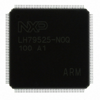
LH79525N0Q100A1;55 NXP Semiconductors, LH79525N0Q100A1;55 Datasheet - Page 25

LH79525N0Q100A1;55
Manufacturer Part Number
LH79525N0Q100A1;55
Description
IC ARM7 BLUESTREAK MCU 176LQFP
Manufacturer
NXP Semiconductors
Series
BlueStreak ; LH7r
Datasheet
1.LH79524N0F100A155.pdf
(64 pages)
Specifications of LH79525N0Q100A1;55
Package / Case
176-LQFP
Core Processor
ARM7
Core Size
32-Bit
Speed
76.2MHz
Connectivity
EBI/EMI, Ethernet, I²C, IrDA, Microwire, SPI, SSI, SSP, UART/USART, USB
Peripherals
Brown-out Detect/Reset, DMA, I²S, LCD, POR, PWM, WDT
Number Of I /o
86
Program Memory Type
ROMless
Ram Size
16K x 8
Voltage - Supply (vcc/vdd)
1.7 V ~ 3.6 V
Data Converters
A/D 10x10b
Oscillator Type
External
Operating Temperature
-40°C ~ 85°C
Processor Series
LH795
Core
RISC
Data Bus Width
16 bit
Data Ram Size
16 KB
Interface Type
I2C, UART
Maximum Clock Frequency
50.803 MHz
Number Of Timers
4
Operating Supply Voltage
3.3 V
Maximum Operating Temperature
+ 85 C
Mounting Style
SMD/SMT
3rd Party Development Tools
MDK-ARM, RL-ARM, ULINK2
Minimum Operating Temperature
- 40 C
Lead Free Status / RoHS Status
Lead free / RoHS Compliant
Eeprom Size
-
Program Memory Size
-
Lead Free Status / Rohs Status
Lead free / RoHS Compliant
Other names
568-4333
935285052557
LH79525N0Q100A1
935285052557
LH79525N0Q100A1
System-on-Chip
Watchdog Timer
against malfunctions. It is a programmable timer to be
reset by software at regular intervals. Failure to reset
the timer will cause a FIQ interrupt. Failure to service
the FIQ interrupt will then generate a System Reset.
The features of the Watchdog Timer are:
• Driven by the bus clock
• 16 programmable time-out periods: 2
• Generates a reset or an FIQ Interrupt whenever a
• Software enable, lockout, and counter-reset mecha-
• Protection mechanism guards against interrupt-ser-
Timers
independently programmable Timer modules. The tim-
ers are clocked by the system clock, but have an inter-
nal scaled-down system clock that is used for the Pulse
Width Modulator (PWM) and compare functions.
scaled counter clock or external clock and can gener-
ate an overflow interrupt. All three timers have separate
internal prescaled counter clocks, with either a com-
mon external clock or a prescaled version of the sys-
tem clock.
• Timer 0 has five Capture Registers and two Com-
• Timer 1 and Timer 2 have two Capture and two Com-
and can generate an interrupt. The Compare Registers
can force the compare output pin either HIGH or LOW
upon a match.
Timer Compare Registers associated with a timer to
create a PWM. Each timer can generate a separate
interrupt. The interrupt becomes active if any enabled
compare, capture, or overflow interrupt condition
occurs. The interrupt remains active until all compare,
capture, and overflow interrupts are cleared.
Preliminary data sheet
clock cycles
time-out period is reached
nisms add security against inadvertent writes
vice failure:
pare Registers.
pare Registers each.
The Watchdog Timer provides hardware protection
– The first WDT time-out triggers FIQ and asserts
– If FIQ service routine fails to clear nWDFIQ, then
The LH79524 and LH79525 incorporate three 16-bit
All counters are incremented by an internal pre-
The Capture Registers have edge-selectable inputs
The timers support a PWM Mode that uses the two
nWDFIQ status flag
the next WDT time-out triggers a system reset.
16
through 2
NXP Semiconductors
Rev. 01 — 16 July 2007
31
General Purpose Input/Output (GPIO)
ble input/output, and the LH79525 provides 86 bits.
Many of the GPIO pins are multiplexed with other sig-
nals. All GPIO feature:
• Individually programmable input/output pins
• All default to Input on power-up.
• LH79524
• LH79525
Boot Controller
device to be used for booting.
• Supports booting from 8-, 16-, or 32-bit devices,
• Configures the byte lane boot state for nCS1,
• Supports booting from alternate external devices
• Glueless interface to external NAND flash.
USB Device
LH79525 is compliant with the USB 1.1 and 2.0 speci-
fication, and compatible with both the OpenHCI and
Intel UHCI standards. The USB Device:
• Supports Full-Speed (12 Mbit/s) operation, and
• Four Endpoints
• Bulk/Interrupt or Isochronous Transfers
• FIFO for each Endpoint direction (except EP0 which
• Supports DMA accesses to FIFO.
selectable via external pins at power-on reset
selectable via external pins at power-on reset.
(e.g., NAND flash) via external pins on power-on reset
suspend and resume signaling
shares a FIFO between IN/OUT). FIFOs exist in
2464 × 8 RAM
The LH79524 provides up to 108 bits of programma-
– Ports A-I, K, L, and N: Bidirectional I/O (Port N is
– Port J: Input only
– Port M: Output only
– Ports A-I: Bidirectional I/O
– Port J: Input only
– Port M: Output only (6 bits wide)
The boot controller allows selection of the hardware
The USB Device integrated into the LH79524/
4 bits wide)
LH79524/LH79525
25


