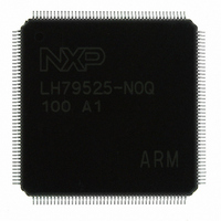
LH79525N0Q100A1;55 NXP Semiconductors, LH79525N0Q100A1;55 Datasheet - Page 44

LH79525N0Q100A1;55
Manufacturer Part Number
LH79525N0Q100A1;55
Description
IC ARM7 BLUESTREAK MCU 176LQFP
Manufacturer
NXP Semiconductors
Series
BlueStreak ; LH7r
Datasheet
1.LH79524N0F100A155.pdf
(64 pages)
Specifications of LH79525N0Q100A1;55
Package / Case
176-LQFP
Core Processor
ARM7
Core Size
32-Bit
Speed
76.2MHz
Connectivity
EBI/EMI, Ethernet, I²C, IrDA, Microwire, SPI, SSI, SSP, UART/USART, USB
Peripherals
Brown-out Detect/Reset, DMA, I²S, LCD, POR, PWM, WDT
Number Of I /o
86
Program Memory Type
ROMless
Ram Size
16K x 8
Voltage - Supply (vcc/vdd)
1.7 V ~ 3.6 V
Data Converters
A/D 10x10b
Oscillator Type
External
Operating Temperature
-40°C ~ 85°C
Processor Series
LH795
Core
RISC
Data Bus Width
16 bit
Data Ram Size
16 KB
Interface Type
I2C, UART
Maximum Clock Frequency
50.803 MHz
Number Of Timers
4
Operating Supply Voltage
3.3 V
Maximum Operating Temperature
+ 85 C
Mounting Style
SMD/SMT
3rd Party Development Tools
MDK-ARM, RL-ARM, ULINK2
Minimum Operating Temperature
- 40 C
Lead Free Status / RoHS Status
Lead free / RoHS Compliant
Eeprom Size
-
Program Memory Size
-
Lead Free Status / Rohs Status
Lead free / RoHS Compliant
Other names
568-4333
935285052557
LH79525N0Q100A1
935285052557
LH79525N0Q100A1
LH79524/LH79525
External DMA Handshake Signal Timing
DREQ TIMING
to HIGH again until after nDACK has been asserted.
44
NOTE: * HCLK is an internal signal provided for reference only.
NOTE: tDREQ0L = DREQ0 LOW Pulse Width = 2 HCLK MIN.
Once asserted, DREQ must not transition from LOW
DEOT0/DEOT1
(See Note)
tDREQ1L = DREQ1 LOW Pulse Width = 2 HCLK MIN.
nBLE[1:0]
nDACK1
DACK0/
D[31:0]
A[23:0]
nWEN
HCLK
nCSx
nOE
Figure 24. Read, from Peripheral to Memory, Burst Size = 1
nDACK1
DREQ0,
DREQ1
DACK0
Figure 23. DREQ Timing Restrictions
NXP Semiconductors
Rev. 01 — 16 July 2007
TRANSITON
MUST NOT
DREQ
TRANSITON
DREQ MAY
DACK/DEOT TIMING
DEOT occur in relation to an external bus access to/from
the external peripheral that requested the DMA transfer.
single read or the last word of a burst read from the
requesting peripheral. The remaining diagrams show
timing for data transfers.
These timing diagrams indicate when nDACK and
The first diagram shows the timing with relation to a
ADDRESS
tDREQ0L,
tDREQ1L
DATA
Preliminary data sheet
System-on-Chip
LH79525-5
LH79525-6


