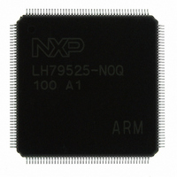
LH79525N0Q100A1;55 NXP Semiconductors, LH79525N0Q100A1;55 Datasheet - Page 29

LH79525N0Q100A1;55
Manufacturer Part Number
LH79525N0Q100A1;55
Description
IC ARM7 BLUESTREAK MCU 176LQFP
Manufacturer
NXP Semiconductors
Series
BlueStreak ; LH7r
Datasheet
1.LH79524N0F100A155.pdf
(64 pages)
Specifications of LH79525N0Q100A1;55
Package / Case
176-LQFP
Core Processor
ARM7
Core Size
32-Bit
Speed
76.2MHz
Connectivity
EBI/EMI, Ethernet, I²C, IrDA, Microwire, SPI, SSI, SSP, UART/USART, USB
Peripherals
Brown-out Detect/Reset, DMA, I²S, LCD, POR, PWM, WDT
Number Of I /o
86
Program Memory Type
ROMless
Ram Size
16K x 8
Voltage - Supply (vcc/vdd)
1.7 V ~ 3.6 V
Data Converters
A/D 10x10b
Oscillator Type
External
Operating Temperature
-40°C ~ 85°C
Processor Series
LH795
Core
RISC
Data Bus Width
16 bit
Data Ram Size
16 KB
Interface Type
I2C, UART
Maximum Clock Frequency
50.803 MHz
Number Of Timers
4
Operating Supply Voltage
3.3 V
Maximum Operating Temperature
+ 85 C
Mounting Style
SMD/SMT
3rd Party Development Tools
MDK-ARM, RL-ARM, ULINK2
Minimum Operating Temperature
- 40 C
Lead Free Status / RoHS Status
Lead free / RoHS Compliant
Eeprom Size
-
Program Memory Size
-
Lead Free Status / Rohs Status
Lead free / RoHS Compliant
Other names
568-4333
935285052557
LH79525N0Q100A1
935285052557
LH79525N0Q100A1
System-on-Chip
AC Test Conditions
Power Consumption By Peripheral Device
individual peripheral device.
Preliminary data sheet
Supply Voltage (VDD)
Core Voltage (VDDC)
Input Pulse Levels
Input Rise and Fall Times
Input and Output Timing
Reference Levels
USB Device (+PLL)
Table 13 shows the typical power consumption by
Ethernet Controller
Table 13. Peripheral Current Consumption
Counter/Timers
LCD Controller
PERIPHERAL
ADC/TSC
UARTs
DMA
RTC
SSP
I
PARAMETER
2
S
REFERENCE
SIGNAL (O)
CLOCK
SIGNAL (I)
TYPICAL
5.6 (+3.3)
OUTPUT
INPUT
590
203
670
200
508
203
4.2
2.2
5.1
Figure 9. LH79524/LH79525 Signal Timing
VSS to VDD
3.0 to 3.6
1.7 to 1.9
RATING
VDD/2
2
tOVXXX
NXP Semiconductors
UNITS
Rev. 01 — 16 July 2007
mA
mA
mA
µA
µA
µA
µA
µA
µA
µA
UNIT
ns
V
V
V
V
AC Specifications
after a reference clock signal. The illustration in Figure
9 represents all cases of these sets of measurement
parameters; except for the Asynchronous Memory
Interface — which are referenced to Address Valid.
• HCLK, the System Bus clock
• PCLK, the Peripheral Bus clock (locked to HCLK in
• SSPCLK, the Synchronous Serial Interface clock
• UARTCLK, the UART Interface clock
• LCDDCLK, the LCD Data clock from the
• and SDCLK, the SDRAM clock.
point of the clock to the 50% point of the signal. See
Figure 9.
(e.g. tOVA) represents the amount of time for the out-
put to become valid from the rising edge of the refer-
ence clock signal. Maximum requirements for tOVXXX
are shown in Table 14.
amount of time the output will be held valid from the ris-
ing edge of the reference clock signal. Minimum
requirements for tOHXXX are listed in Table 14.
amount of time the input signal must be valid before the
rising edge of the clock signal. Minimum requirements
for tISXXX are shown in Table 14.
amount of time the output must be held valid from the
rising edge of the reference clock signal. Minimum
requirements are shown in Table 14.
tISXXX tIHXXX
the LH79524/LH79525)
LCD Controller
All signals described in Table 14 relate to transitions
The reference clock signals in this design are:
All signal transitions are measured from the 50%
For outputs from the LH79524/LH79525, tOVXXX
The signal tOHXXX (e.g. tOHA) represents the
For Inputs, tISXXX (e.g. tISD) represents the
The signal tIHXXX (e.g. tIHD) represents the
tOHXXX
LH79524/LH79525
LH79525-28
29


