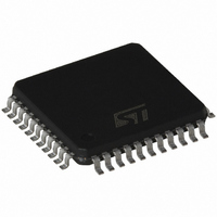
ST72F361J9T6 STMicroelectronics, ST72F361J9T6 Datasheet - Page 132

ST72F361J9T6
Manufacturer Part Number
ST72F361J9T6
Description
IC MCU 8BIT 60K FLASH 44-LQFP
Manufacturer
STMicroelectronics
Series
ST7r
Datasheet
1.ST72F361K6T6.pdf
(225 pages)
Specifications of ST72F361J9T6
Core Processor
ST7
Core Size
8-Bit
Speed
8MHz
Connectivity
LINSCI, SPI
Peripherals
LVD, POR, PWM, WDT
Number Of I /o
32
Program Memory Size
60KB (60K x 8)
Program Memory Type
FLASH
Ram Size
2K x 8
Voltage - Supply (vcc/vdd)
3.8 V ~ 5.5 V
Data Converters
A/D 16x10b
Oscillator Type
External
Operating Temperature
-40°C ~ 85°C
Package / Case
44-LQFP
Processor Series
ST72F3x
Core
ST7
Data Bus Width
8 bit
Data Ram Size
2 KB
Interface Type
LINSCI, SPI
Maximum Clock Frequency
8 MHz
Number Of Programmable I/os
34
Number Of Timers
2
Maximum Operating Temperature
+ 85 C
Mounting Style
SMD/SMT
Development Tools By Supplier
ST72F36X-SK/RAIS, STX-RLINK
Minimum Operating Temperature
- 40 C
On-chip Adc
10 bit, 11 Channel
Lead Free Status / RoHS Status
Lead free / RoHS Compliant
Eeprom Size
-
Lead Free Status / Rohs Status
Details
Available stocks
Company
Part Number
Manufacturer
Quantity
Price
Company:
Part Number:
ST72F361J9T6
Manufacturer:
STMicroelectronics
Quantity:
50
Company:
Part Number:
ST72F361J9T6
Manufacturer:
STMicroelectronics
Quantity:
10 000
ST72361
LINSCI™ SERIAL COMMUNICATION INTERFACE (SCI Mode) (cont’d)
CONTROL REGISTER 2 (SCICR2)
Read/Write
Reset Value: 0000 0000 (00 h)
1)
Bit 7 = TIE Transmitter interrupt enable
This bit is set and cleared by software.
0: Interrupt is inhibited
1: In SCI interrupt is generated whenever
Bit 6 = TCIE Transmission complete interrupt ena-
ble
This bit is set and cleared by software.
0: Interrupt is inhibited
1: An SCI interrupt is generated whenever TC = 1
Bit 5 = RIE Receiver interrupt enable
This bit is set and cleared by software.
0: Interrupt is inhibited
1: An SCI interrupt is generated whenever OR = 1
Bit 4 = ILIE Idle line interrupt enable
This bit is set and cleared by software.
0: Interrupt is inhibited
1: An SCI interrupt is generated whenever
Bit 3 = TE Transmitter enable
This bit enables the transmitter. It is set and
cleared by software.
0: Transmitter is disabled
1: Transmitter is enabled
Notes:
– During transmission, a “0” pulse on the TE bit
– When TE is set there is a 1 bit-time delay before
Bit 2 = RE Receiver enable
This bit enables the receiver. It is set and cleared
by software.
0: Receiver is disabled in the SCISR register
132/225
refer to the LIN mode register description.
This bit has a different function in LIN mode, please
(“0” followed by “1”) sends a preamble (idle line)
after the current word.
the transmission starts.
TIE
TDRE = 1 in the SCISR register
in the SCISR register
or RDRF = 1 in the SCISR register
IDLE = 1 in the SCISR register.
7
TCIE
RIE
ILIE
TE
RE
RWU
1)
SBK
0
1)
1: Receiver is enabled and begins searching for a
Bit 1 = RWU Receiver wake-up
This bit determines if the SCI is in mute mode or
not. It is set and cleared by software and can be
cleared by hardware when a wake-up sequence is
recognized.
0: Receiver in active mode
1: Receiver in mute mode
Notes:
– Before selecting Mute mode (by setting the RWU
– In Address Mark Detection Wake-Up configura-
Bit 0 = SBK Send break
This bit set is used to send break characters. It is
set and cleared by software.
0: No break character is transmitted
1: Break characters are transmitted
Note: If the SBK bit is set to “1” and then to “0”, the
transmitter will send a BREAK word at the end of
the current word.
DATA REGISTER (SCIDR)
Read/Write
Reset Value: Undefined
Contains the Received or Transmitted data char-
acter, depending on whether it is read from or writ-
ten to.
The Data register performs a double function (read
and write) since it is composed of two registers,
one for transmission (TDR) and one for reception
(RDR).
The TDR register provides the parallel interface
between the internal bus and the output shift reg-
ister (see
The RDR register provides the parallel interface
between the input shift register and the internal
bus (see
DR7
bit) the SCI must first receive a data byte, other-
wise it cannot function in Mute mode with wake-
up by Idle line detection.
tion (WAKE bit = 1) the RWU bit cannot be mod-
ified by software while the RDRF bit is set.
start bit
7
DR6
Figure
Figure
DR5
1).
1).
DR4
DR3
DR2
DR1
DR0
0


